This thread has been locked.

If you have a related question, please click the "Ask a related question" button in the top right corner. The newly created question will be automatically linked to this question.

TPS23731: Please help confirm if this current value is normal

Part Number: TPS23731
Other Parts Discussed in Thread: TPS23734,

Tool/software:

Dear Expert

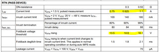
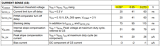
Hello, my PoE device uses the TPS23734 chip and measures an input current of approximately 19mA during standby mode. The waveform is attached. Could you please help confirm if this current value is normal? Thank you!

idle current.zip

  • Hi Gabriel,

    Thanks for reaching out. 19mA could be a correct value. I recently tested a TPS23731 based reference design has 12mA stand by current at 48V input and open load output. If no issues at output, it could be normal. 

    Best regards,

    Diang

  • Dear Sir

    okay, thank you
    Today during debugging, I encountered a problem. Could you please help me answer it? In at mode, Rcls=31.6ohm, when the input is 42V, the OCP value of the prototype output 9V is 2.5A, which is equivalent to an output power of 9 * 2.5=22.5W. However, when the input is adjusted to 57V, the OCP value of the prototype output 9V is 3.5A, which is equivalent to an output power of 9 * 3.5=31.5W. What is the protection mechanism of this classification? Why do there be different powers at different voltages, even exceeding the maximum value of 25.5W? My understanding should be that the same power value is correct, regardless of the input voltage. When measuring the above OCP, the CS voltage of pin1 is about 0.12V, and the current limiting protection of the main MOS is not triggered.

  • Today is holiday in USA please allow some time to get back to you. 

  • Hi Gabriel,

    There are multiple elements are related to the OCP:

    1. When a PSE-PD make the classification. The PSE will set a power cut threshold, For example, if 30W Pcut is set for Class-4, when the PSE output power exceed this value the PSE could turn off the port.

    2. The TPS23731 has foldback protection on its internal hotswap between RTN and VSS. This current limiting is fixed as 0.75 - 1.1A. This is related to current. 

    3. The CS pin can also help to configure over current protection. But we do not always want to make it close to the power limit since your feedback loop may be compromised. This is related to the current too. You can reduce the CS resistor to allow sufficient power at a lower Vin. 

    Best regards,

    Diang

  • Dear Diang

    Today during debugging, I encountered a problem. Could you please help me answer it? In at mode, Rcls=31.6ohm, when the input is 42V, the OCP value of the prototype output 9V is 2.5A, which is equivalent to an output power of 9 * 2.5=22.5W. However, when the input is adjusted to 57V, the OCP value of the prototype output 9V is 3.5A, which is equivalent to an output power of 9 * 3.5=31.5W. What is the protection mechanism of this classification? Why do there be different powers at different voltages, even exceeding the maximum value of 25.5W? My understanding should be that the same power value is correct, regardless of the input voltage. When measuring the above OCP, the CS voltage of pin1 is about 0.12V, and the current limiting protection of the main MOS is not triggered

  • Hi Gabriel,

    Thanks for your reply. 

    It is normal and it could be related to the CS pin. You can put a 750k resistor (or other resistance) between VDD to CS to compensate. 

    At the same power, when you have a higher input voltage, your current ramping point is lower. So the CS is less like to trigger the CTL line in peak current mode control.

    In most of time, we won't rely on CS pin to do over current protection. Though it will help to protect in some conditions. TPS23731's VSS-RTN hotswap FET foldback protection is where we do over current protection. 

    Best regards,

    Diang