A related question is a question created from another question. When the related question is created, it will be automatically linked to the original question.
If you have a related question, please click the "Ask a related question" button in the top right corner. The newly created question will be automatically linked to this question.
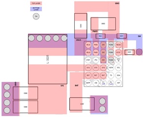
The switching node rise and fall times should be minimized for minimum switching loss. Proper layout of the components to minimize high frequency current path loop is important to prevent electrical and magnetic field radiation and high frequency resonant problems. Follow this specific order carefully to achieve the proper layout.
1. Place input capacitor as close as possible to PMID pin and GND pin connections and use shortest copper trace connection or GND plane.
2. Place inductor input pin to SW pin as close as possible. Minimize the copper area of this trace to lower electrical and magnetic field radiation but make the trace wide enough to carry the charging current. Do not use multiple layers in parallel for this connection. Minimize parasitic capacitance from this area to any other trace or plane.
3. Put output capacitor near to the inductor and the device. Ground connections need to be tied to the IC ground with a short copper trace connection or GND plane.
4. Place decoupling capacitors next to the IC pins and make trace connection as short as possible.
5. Ensure that the number and sizes of vias allow enough copper for a given current path.