This thread has been locked.

If you have a related question, please click the "Ask a related question" button in the top right corner. The newly created question will be automatically linked to this question.

LMG5200: IC heating on our product far exceeding what's seen on the eval board

Part Number: LMG5200

Tool/software:

This has been kicking us in the butt for a while so, here i go........

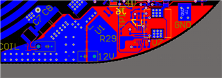
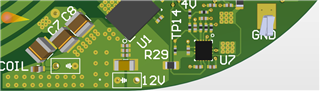
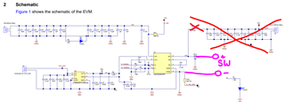
  1. We are designing a new product that uses the LMG5200 to drive an LC tank at resonance.
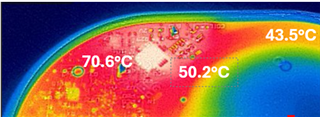
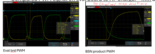
  2. When putting out ~ 6-7 Watts of power we see excessive heating in the order of 70C on the IC.
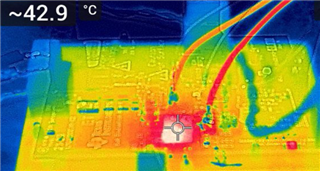
  3. When driving the same load and same power output using the Eval board we see around 40C.


So our natural question is, what’s causing the heating difference. We have tried a few board iterations and have reduced the temp by 20C but we still far off from the eval board.

  • Hello,

    I have a few questions that will help us get the ball rolling with possible ideas:

    - The thermal situation with your board from the copper layers of your PCB, is there any way you can share this information? Maybe the heat is not spreading in your PCB well causing a large buildup

    - How are you measuring the temperature?

    - Can you share more details about the "6-7W" of power, is this device losses? It would be helpful if you could give me input and output voltage/current.

    - I assume you are using this EVM:https://www.ti.com/tool/LMG5200EVM-02 how do you have it configured? And how exactly are the two tests similar and different?

    Thanks,

    Zach

  • Thanks for the reply Zach. 

    1. the layout has a copper pour connected to the GND pin and another for Vin. the copper pour on GND has a few dozen stitching vias connecting it to the other side of the PCB were another larger copper pour exists. (Blue pour on top layer, Red pour is on bottom layer)

    the top copper pour as an area of 0.273 in^2

    the bottom copper pour has an area of 0.773 in^2

    Adding these copper pours reduced the heat by about 10C. We have also tried using a Rogers PCB which dropped the temp by another 10C.This does point to possibly needing larger pours. The Eval board does have larger copper pours.. However, as you can see in the image below it appears the heat is wicking away into the PCB quite well .

    2. were measuring the heat with a FLIR IR camera. 

    3. the power is measured via the power supply that powers Vin on the IC. 

    4. Yes, im using the LMG5200EVM-02. Using two channels for the power supply to power the IC logic and the Vin seperately. This is also done on our PCBA to give a one to one comparison. 

    On our PCBA the LMG5200 is driving the load on the same pcb. When using the eval board the output of the LMG5200 is wired to drive the load on our PCBA so that the load is essentially the same (minus the long wires connecting 2 boards.

    The eval board is using a single channel input from a function generator to drive the on board logic that creates the actual PWM (HI and LO) signals.

    Ive compared the PWM signals coming from our uC with the output of the Logic circuit on the eval board and they look very similar, i.e. rise time, dead time , frequency and duty cycle.

  • Hello Johnathan,

    Apologies for the late response, the US holiday has made me delayed.

    Thank you for the pictures and explanation, I believe I have a good idea of how the two circuits are configured, allow me to share my thoughts and you can fill in any missing or incorrect details.

    1. The LMG5200 EVM has the SW output connected to your board as follows (from my understanding):

    So from my understanding you removed the SW inductor and output caps and just routed the whole SW over to your custom PCB with wires. You can plug or unplug the EVM to control which board (custom or EVM) is used for the system.

    2. You have verified that the PWM signals are very similar. This is what I first thought would be an issue, perhaps with deadtime or some improper turn-on/turn-off. Based on the LC tank configuration I assume the LMG5200 device is fully soft switched?

    3. Can you help share details about the switching waveforms for this configuration? Ideally if you are able to share SW voltage and current waveform that would be ideal. I have seen instances where "jumping" one PCB to another can cause excessive parasitics and ringing, but that would lead me to think that the EVM part would get warmer.

    4. Can you also share the slew rate for your PCB? ideally it would help to see your full schematic and try to match-up to the EVM, if you are able to share that would be great but if not we can try and work around.

    Thanks,

    Zach

  • No worries about time. I appreciate any time you can give. 

    You are correct, i have removed the SW inductor and output caps to drive the external load. 

    I have verified the PWM signals are very similar. I adjusted the uC PWM to match the dead time and pulse widths. Rise times are less then 5% off of each other. 

    the Switch node voltages are somewhat different. the slew rate on our product board is (10V / 2.6nS). the eval board is less then half of that. 

    I would add the scope capture but im having issues pasting it here.... 

    Ill have to work on getting the current waveforms.

  • Thank you for the updated information,

    This may be a long shot, but right now I am looking into the thermal resistance difference between the 4 layer board used in the EVM and the 2 layer PCB you shared with me.

    I have experience with poor bottom-side cooling and the temperature difference can be quite large. Even with a decent amount of stitching vias, it is the largest difference I see at the moment. As I look into this, if you have any information about the thermal resistance of your PCB let me know.

    Thanks,

    Zach

  • My design is 4 layers i just have the 2 inner ground planes hidden to visualize the top and bottom layers. 

    But, this comment does resonate with our thoughts here. One of the proposed layout changes Is to move the IC to the other side of the pcb so that we can increase the size of the copper pours connected to power ground and VDD. The thought was that the copper connected to those pins will wick away heat much better then a bottom side plane connected with vias. 

    I greatly appreciate the help and all your thoughts. I think after all the troubleshooting we have done on our end and the discussion I am concluding the most likely culprit is the inability to dissipate heat on the top layer. 

    I will be certain to update this thread with our solution once we have it.