This thread has been locked.

If you have a related question, please click the "Ask a related question" button in the top right corner. The newly created question will be automatically linked to this question.

LP876242-Q1: Reference Design Issue

Part Number: LP876242-Q1

Tool/software:

Hi team,

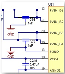
My customer is using our LP876242-Q1 and looks at our reference design.

And they have two questions about our reference design:

1. Why should PIN17 and PIN25 of PMIC be directly connected to 1.2V and 5V power supply? Datasheet defines these two ports as normal GPIO I/O.

2. What is the role of Murata NFM18HC105C1C3 in the reference design? Why is this particular capacitor chosen?

Thanks a lot!

Best Regards,

Matt.

  • Hi Matt.

    1. PIN17 monitors the output voltage of BUCK2 after the filter. And PIN25 monitors the external Boost 5V output voltage. Those pins are configured in the NVM as VMONs (voltage monitors). 

    3. That's three terminal input filtering capacitance. You can use 2 terminal capacitance as well. 3T cap has been seen more efficient than 2T cap. That's why it is recommended however, it is not mandatory customer can choose to use 2T cap and they also work pretty fine.

    Regards,

    Ishtiaque