This thread has been locked.

If you have a related question, please click the "Ask a related question" button in the top right corner. The newly created question will be automatically linked to this question.

LM5012-Q1: LM5012 intermittent operation

Part Number: LM5012-Q1
Other Parts Discussed in Thread: LM5012

Tool/software:

Hi to all,

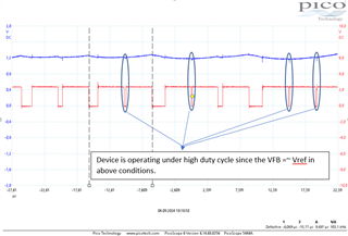
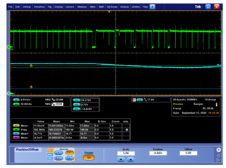
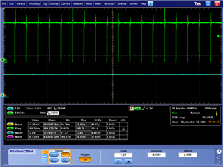
i did a new design with LM5012 which works mostly fine. The only issue is, that the circuits switch to an intermittent operation after a while (see oszi picture below, 10:1 divider) at a input voltage of 19,2...19,5V. This happens after 15min operation, so i think it's an temperature issue? When cold, most circuits are working correctly even at 17,5V input voltage. The "warm" circuits are operating correctly at a voltage of 22V, which ist too high.

Data:

Uin: 19,2V to 57,6V

Uout: 18V

Iin: 500mA at 24V Uin

Switching frequency: 200KHz

Looking forward for some helping hints - thanks in advance

PODIS FEHLER 01.pdf

PODIS-V01_SLP.pdf

PODIS-V01_LAY.pdf

  • Hello,

    It's possible your 47pF coupling cap (C11) on the ripple injection circuit is losing capacitance at hot and getting discharged by the 49.9kΩ lower feedback resistor. Try 100-220pF here instead to see if that helps the operation near dropout.

    Regards,

    Tim

  • Hello Timothy,

    thank you for your reply. I tried 100p and 220p. Both improved the regulation at 19V (better, but not very good).  But now regulation at 24V is worse. Also voltage regulation is worse (18.2V at 24V Vin, 19.1V at 48V Vin). Please see the attached oszi pictures. First is 19V, second is 24V. With 100p populated, regulation becomes good at about 36V. With 220p populated regulation is not good over the whole range.

    Regards

    Norbert

    PODIS_GOOD_19V.pdf

    PODIS_FAIL_24V.pdf

  • Norbert,

    Check the injected ripple amplitude, as a COT converter will regulate at the bottom of the ripple. Thus, the DC output voltage rides higher by half the ripple amplitude.

    Tim

  • Hi Tim,

    please see attached the ripple waveform, measured at PIN5 of LM5012. C11 is populated with 100p.

    PODIS_FAIL_02_24V.pdf

  • Hi Nobert,

    Thanks for the FB voltage waveform along with SW node. Based on the waveform, the device is operating in high duty cycle due to incorrect ripple at the FB pin. Can you double check the ripple generation components or can you increase the ripple voltage to say >30mV by varying RA, CB, CA values. 

    Thanks,

    Nitya

  • Hi Nitya.

    thanks for you reply. I tried some variations on the ripple network:

    RA: 137K, CA: 3n3, CB: 100p. This was from the picture above

    RA: 340K, CA: 3n3, CB: 100p. ok up to 19.4V, then worse

    RA: 88K7, CA: 3n3, CB: 100p. Better, gets worse when warm (about 45°C)

    RA: 88K7, CA: 4n7, CB: 100p. Bad

    RA: 88K7, CA: 2n2, CB: 100p. Very good when it's cold, bad up to 19.9V when it's warm. Very good from 20V up.

    The issue is the range from 19V to 20V. Unfortunatelly the circuit has to work from 19.2V up.

    Another problem is, that in all constellations, the output voltage moves from 18.3V to 20V (While driving input voltage from 19.2V to 57V)?

    Do you have a hint, what values of the ripple components would be good? What are the borders? Should i make the output voltage divider more low ohmic? How significant is the used material of the capacitors? Every hint to get this work, would be helpful!

    Here are 3 oszi pictures.

    18V9_good.pdf

    19V7_bad.pdf

    24V_good.pdf

    Kind regards

    Norbert

  • Hi Nitya,

    in addition to my post from yesterday i found this application note from TI.

    CB is there 2u2. Would this be a option? Or should i change switching frequency?

    Kind regards

    Norbert

  • Hi Nobert,

    Let me check the above condition on EVM and get back to you tomorrow with component values. 

    Thanks,

    Nitya

  • Hi Nitya,

    i played around with some more changes.

    RA: 88K7, CA: 2n2, CB: 560p, RFB1: 150K, RFB2: 11K seems to be a relative stable configuration. Except a jitter at 19.4V

    Generally, making CA higher seems to make the circuit more instable.

    But as in all configs, the output voltage climps from 18V to 20V (Vin: 19.2V to 50V)

    Kind Regards

    Norbert

  • Hi Nobert,

    Did you capture the waveform when output voltage clips when VIN is 19.2V to 50V?, If yes, can you share those waveforms?

    Thanks,

    Nitya

  • Hi Nitya,

    sorry for my english, but the output voltage does not clip. It moves up steadily with the input voltage. At 19.2V input there are 18V output (as wanted), and at 50V input there are 20V output voltage.

    What waveform do you want to see? Could you check the values and the behaviour of CA (see my last post, bigger CA makes more instability)?

    Regards

    Norbert

  • Hi Nobert,

    Now it is clear to me what you wanted to convey. But why the output voltage is settled to 20V when input is higher? Can you doble check the values. 

    I am trying to reproduce the issue around 19.2V, I checked basic behavior and i see output voltage is pretty stable at 19.2V. Let me capture some waveforms today and get back to you. 

    BTW, 19.2V did you measure right at the input of the buck converter or the power supply reading? If it power supply reading, then at the device input the voltage is lower due to resistive drop. Recommend you to measure the voltage right across the input capacitor of device.

    Thanks,

    Nitya

  • Hi Nobert,

    I believe you are measuring the power supply input voltage and not the voltage across the input of the device. We have repeated the experiment on EVM. We are seeing the similar behavior at lower voltage around 18.6V but at 19.2V input, the device is operating as expected. 

    1. Test Conditions: VIN = 18.5V, Vout: 17.7V(output voltage setting), Iout=500mA

    2. Test Conditions: VIN =19.2V, Vout : 17.7V(output voltage setting), Iout=500mA

    Ra : 89k, Cb:470p and Ca=2.2nF.

    Thanks,

    Nitya   

  • Hi Nitya,

    thank you for your measurement - i will check the voltage drop from the power supply to the circuit.

    Could you also check, why Uout is going up while Uin is going up? (Uout: 18V to 20V by Uin = 19,2V to 50V)

    Are the values for RA, CB, CA in a good range? Are there rule of thumb recommendations?

    I found out, that the output ceramic capacitors (2x 22uF) caused some trouble, since there capacitive ripple was higher then the ripple of the RA/CA/CB network. I replaced with a 22uF tantalum and behaviour at low voltage is much better.

    Regards

    Norbert

  • Hi Nobert,

    Can you check the feedback resistor values? and if you have the waveforms during start-up it would be helpful. 

    Regarding the selection of Ra, Ca, and Cb values recommend you to refer app note: snva776a

    Thanks,

    Nitya

  • Hi Nitya,

    sorry, but i have to come back to this once more.

    By replacing the output capacitor with a 22uF tantalum, i could use 7 of 10 boards without failure.

    3 boards showing this signal (below) at 19.2V input voltage (measured at input capacitor).

    RA: 137K, CA: 3n3, CB: 47p

    Moving CB to 100p without change in waveform.

    Can you explain me, in what mode the IC is there and what to do, to get it as the other boards?

    20240917-0001.pdf

    Kind regards

    Norbert

  • Hi Nobert,

    I would check the feedback voltage along with switch node in both fail and pass devices to check if the feedback voltage is as expected. If the injected signal is as expected, then it is LM5012 issue else we need to check injected ripple components derating values.

    Thanks,

    Nitya