Tool/software:
Hello! As it says in the title I've been trying to make an active Sodium-Ion ESP32 active battery balancer using the UCC27282-Q1 for the past couple of months. I came up with 2 different versions, none of which I am sure are wired accordingly or that they work. Could you please tell me how I should wire the IC to the MOSFETS or if the IC is even for this application as it says it can do half bridge.
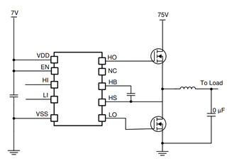
The project was inspired by this video where it explains a basic schematic of the battery balancer at 6:24:How Does An Active Balancer Work? (youtube.com). Also here's the schematic from the video which I tried to copy but I just don't know where the HO and LO pins should be, which ones are high and which ones are low, and whether there must be 1 driver/ each 1 pair (from right to left), so essentially the number of drivers would be (number of mosfets/2)
OR if there should be 1 driver/ battery. One battery has 2 bottom and 2 top so each pin gets 2 mosfets therefore a driver will have 4 mosfets assigned to it, not 2, therefore number of drivers = number of batteries
Also where are we supposed to connect the DS pin? to the negative part of the capacitors or to the positive?
See the designs and if you could draw or tell me how to do it that would be HEAVILY appreciated! Is any of these 2 designs right?
As far as I understood flying capacitors work in 2 phases:
1. Connect capacitors to batteries in parallel (bottom MOSFETs activated, top deactivated)
2. Connect capacitors in parallel (bottom MOSFETs deactivated, top activated)
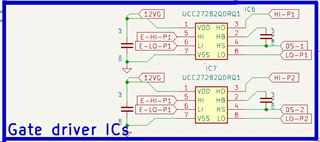
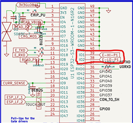
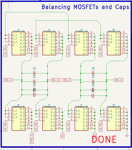
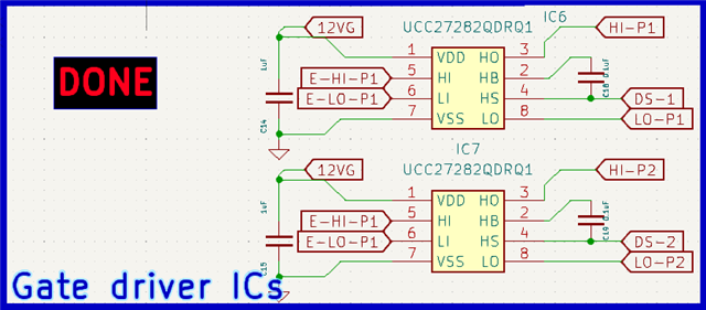
-In both designs, E-HI-P1 and E-LI-P1 are controlled by an ESP32 digital pin. E-HI-P1 controls all the "HIGH" side driver inputs "HI", and E-LI-P1 controls all the "LOW" side driver inputs "LI".
-GND is battery negative. P1/2/P2S-E/... mean battery positive 1/positive 2. (Both designs are for a 2S battery balancer)
-Also all drivers have been driven by an ESP32 or Arduino UNO
Here's the schematic of the first design:
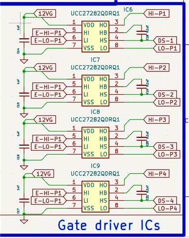
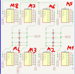
Here each driver controls 1 pair of mosfets, therefore 4 drivers. It made more sense because that way I could connect DS-1 to line GND, DS2 to line P1, DS3 to line P1 and DS4 to line P2.
Results with this design:
- 1 X board seemed to have succesfully balanced out a approx 1V difference between 2 batteries in like 24 hours. (small switching frequency), cool
- 1 X board on fire (may have been my mistake with some MOSFETs having bad connections)
- 3 X boards not tested thoroughly
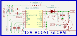
Here's the schematic of the second design:
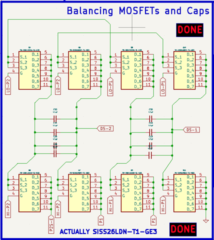
Here I used HO and LO each driving 2 mosfets so 4 in total, 1 driver per 4 mosfets. But which is which? Which is HIGH side and which is LOW side? I also didn't know where to place DS so I just placed it on the GND line (when the capacitors are placed in parallel)
Results:
- 1 X board today, nothing on fire, but didn't seem to balance even 1mV in 15 min, switching frequency 500Hz, 1V difference between batteries