This thread has been locked.

If you have a related question, please click the "Ask a related question" button in the top right corner. The newly created question will be automatically linked to this question.

BQ2970: Is there a risk of causing a path for leakage if using dual BQ2970?

Part Number: BQ2970

Tool/software:

Hi,

There is a worry that one could end up in a state with additional leakage using dual BQ2970 for dual protection. Will try to explain the reasoning, to get your thoughts on this.

In chapter 8.4.4 of the BQ2970 datasheet the following is stated:

"In the discharge overcurrent status, the V– and VSS pins are connected by a constant current sink I_V–S. When this occurs and a load is connected, the V– pin is at BAT potential. If the load is disconnected, the V– pin goes to VSS (BAT/2) potential.

The resistance R_V–D between V– and BAT is not connected in the discharge overcurrent detection status."

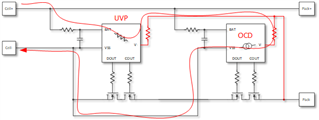
Some PCMs implement dual protection (for single fault handling) by simply duplicating the safety IC and discharge/charge FETs, in series. Both ICs' V- pins are then connected to the same PACK- node (through their own 2.2k). If over-discharge is detected by an IC, that IC's V- pin will be pulled to BAT potential through the internal R_V–D.
See schematic below.

Questions:

1) When one IC enters over-discharge status, is it a risk that this pull of that IC's V- pin to BAT can trigger discharge overcurrent status for the other IC, by pulling the V- pin of that other IC high, before it has detected over-discharge itself?

2) If one IC enters over-discharge status and the other IC enters discharge overcurrent status, is there a risk there would be leakage due to the current path IC1 BAT > IC1 V- > IC2 V- > IC2 VSS, as shown with the red arrow in the schematic?

3) Or is this a case that will simply not happen (IC1 over-discharge pulling IC2 V- to generate a false IC2 discharge overcurrent status and leakage path)? For instance due to R_V-D being ~300kOhm so that the V- node will be BAT - 1V already at 1/300k = 3.3 uA, which is less than the minimum current of the I_V-S sink, causing IC2 to leave an discharge overcurrent status if it ever happened in the first place?

4) In the text "the V– pin goes to VSS (BAT/2) potential." Assuming those potentials are referenced to Pack-, can you elaborate on how come VSS = BAT/2? Is this referring to when restored to normal status or not (considering that BAT/2 < BAT - 1V which releases the discharge overcurrent status)?

5) If multiple conditions occur (such as discharge overcurrent and over-discharge) during a period, is it simply so that the one that occurs first in time wins and then the IC stay with that status until it is released due to the described release conditions for that state? Or does any other priority excist?

  • Hello Southern Engineer,

    These are some good questions. Let me think through it some and I will give you an answer by Friday (Apologies for the wait, tomorrow we are packed).

    Best Regards,

    Luis Hernandez Salomon

  • Hello Southern Engineer,

    1) When one IC enters over-discharge status, is it a risk that this pull of that IC's V- pin to BAT can trigger discharge overcurrent status for the other IC, by pulling the V- pin of that other IC high, before it has detected over-discharge itself?

    I think that sounds possible.. But I will talk with our designer to see what he thinks on this.

    ) If one IC enters over-discharge status and the other IC enters discharge overcurrent status, is there a risk there would be leakage due to the current path IC1 BAT > IC1 V- > IC2 V- > IC2 VSS, as shown with the red arrow in the schematic?
    3) Or is this a case that will simply not happen (IC1 over-discharge pulling IC2 V- to generate a false IC2 discharge overcurrent status and leakage path)? For instance due to R_V-D being ~300kOhm so that the V- node will be BAT - 1V already at 1/300k = 3.3 uA, which is less than the minimum current of the I_V-S sink, causing IC2 to leave an discharge overcurrent status if it ever happened in the first place?

    This also sounds possible. 

    4) In the text "the V– pin goes to VSS (BAT/2) potential." Assuming those potentials are referenced to Pack-, can you elaborate on how come VSS = BAT/2? Is this referring to when restored to normal status or not (considering that BAT/2 < BAT - 1V which releases the discharge overcurrent status)?

    When the load is connected, it pulls PACK minus to the BAT potential (Since PACK- is not connected to Vss). When the load is removed PACK- is then left floating connected solely to the current source from V-. It is likely that this BAT/2 is just the voltage that the current source would generate in the case when PACK- is left floating.

    5) If multiple conditions occur (such as discharge overcurrent and over-discharge) during a period, is it simply so that the one that occurs first in time wins and then the IC stay with that status until it is released due to the described release conditions for that state? Or does any other priority excist?

    Another great question. I would imagine there is a priority. But it is also something I will have to confirm with the designer.

    Apologies for the long wait on these answers! Will message our designer about it today.

    Best Regards,

    Luis Hernandez Salomon