Other Parts Discussed in Thread: LM5161
Tool/software:
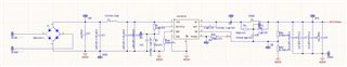
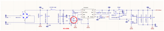
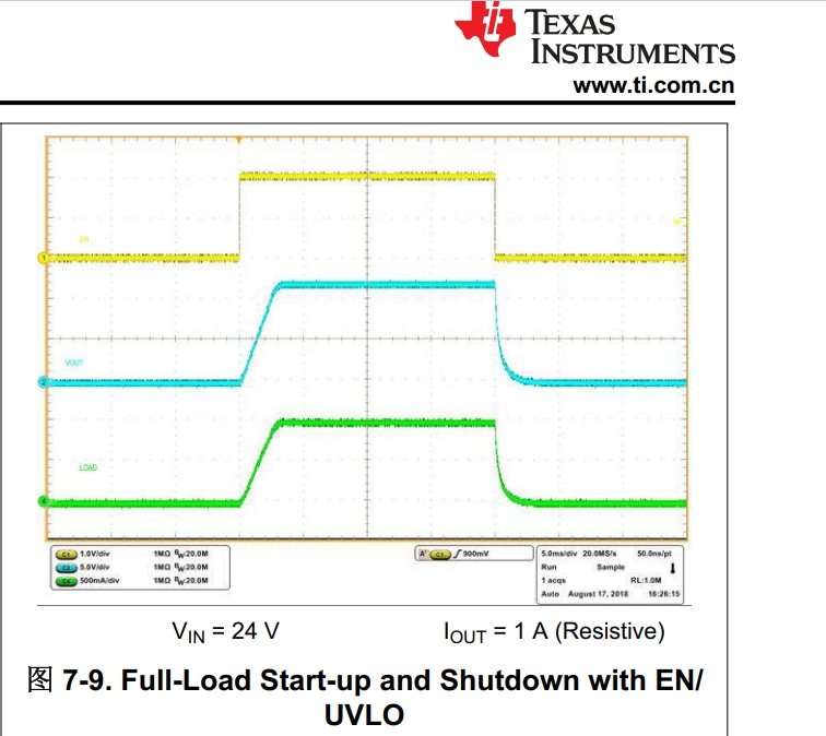
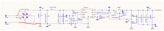
As shown in Fig
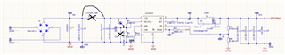
It is planned to design a power supply, the input voltage is: 9V~40V support (maximum AC28V input), and the output is: 8V@0.4A.
The 220uH inductor is designed to allow the LM5164 to operate in CCM mode at the time of the output 8V@40mA.
9V-40V is ideally operated in CCM mode, and the output ripple is also within the design range.
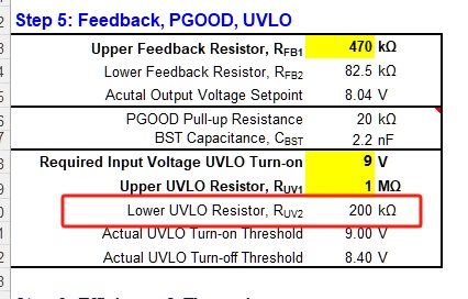
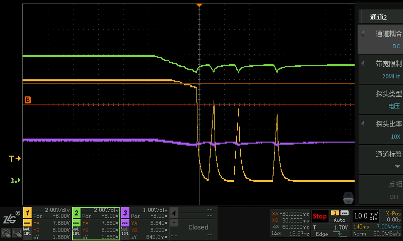
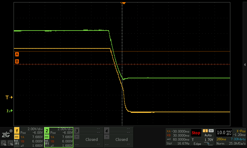
However, when the input input is turned off, the output waveform is detected as shown in the following figure, the yellow waveform is the output, and when the input voltage is turned off (green), the 8V output will be glitched when the output supply voltage drops (the load is 20ohm false load)
Figure 1 shows the input DC40V (AC28V) waveform with the input voltage test turned off, and the output voltage waveform is yellow..
(The green waveform is the input voltage, please ignore the fluctuating DC voltage after rectification filtering)
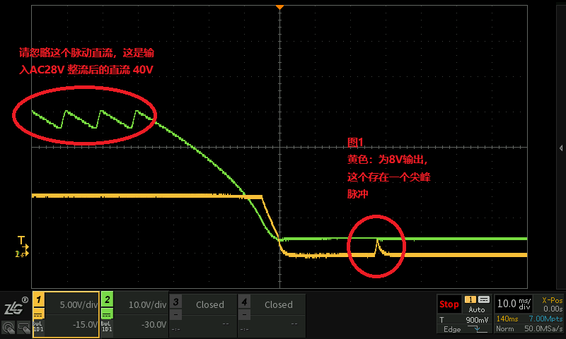
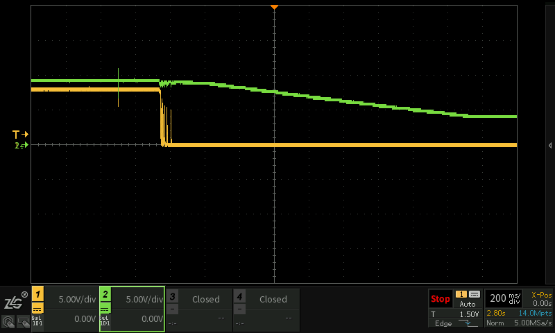
Figure 3 As shown below, when the input voltage is turned off at DC24V, there is a spike in the output voltage waveform. (Output waveform is yellow: DC8V)
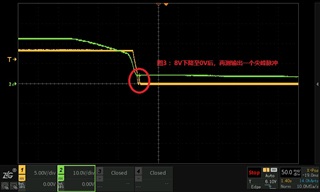
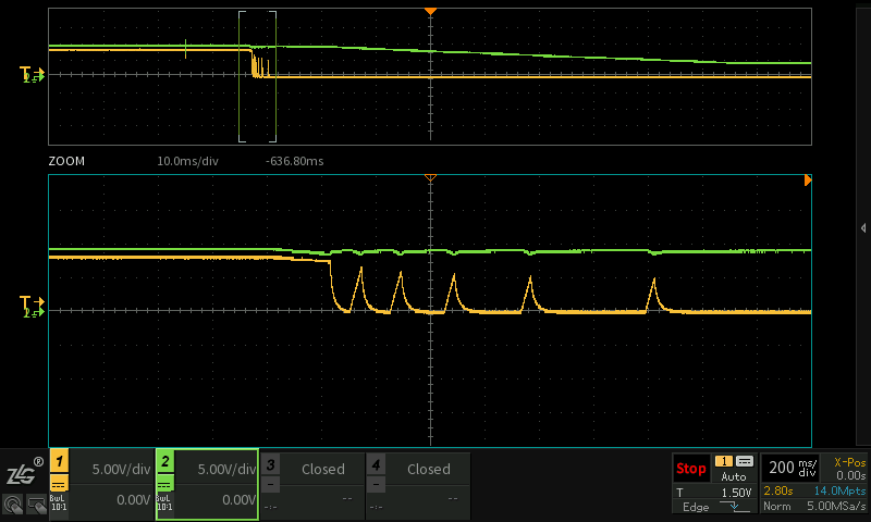
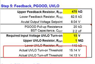
Figure 4 As shown below, when the input voltage is turned off at 12 VDC, there are multiple spikes in the output voltage waveform. (Output waveform is yellow: DC8V)
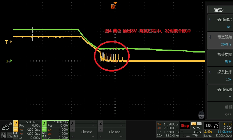
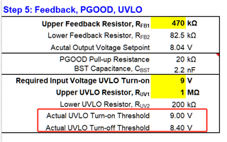
Figure 5 As shown below, when the input voltage is turned off at DC9V, there are multiple spikes in the output voltage waveform. (Output waveform is yellow: DC8V)

I want to know:
1. How to eliminate this pulse during the output drop process;
2. What is the reason for this situation?
Thank you so much..