This thread has been locked.

If you have a related question, please click the "Ask a related question" button in the top right corner. The newly created question will be automatically linked to this question.

UCC28711: UCC28711

Part Number: UCC28711

Tool/software:

Hello! I have created an SMPS based on the document "400- to 690-V AC Input 50-W Flyback Isolated Power Supply Reference Design for Motor Drives."

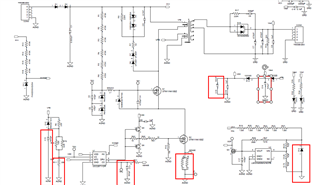
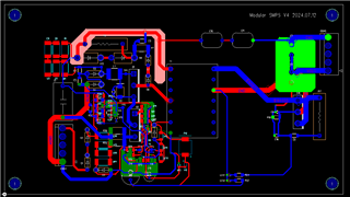
The schematic is as follows, and the PCB layout was done in the same way.

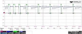
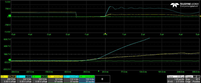
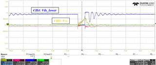
I followed the guide to create it, and I am currently testing it. So far, I have confirmed an output of 1 A with 600 Vdc input (refer to Figures 1 and 2). However, I have some concerns, so I cannot raise the voltage further in my experiment.

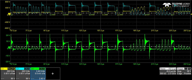
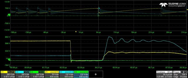
  1. The document explains the following: At lower voltages (when upper switch Zener V < Vin), Figure 19 shows no ringing in Vds. However, in my experiment waveform, I see ringing (refer to Figure 3).

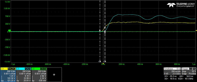
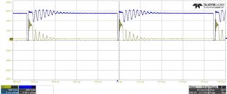
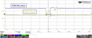
  2. The SMPS designed according to the guide starts operating at 400 Vdc input, and this also happens in my experiment. However, when I connect the oscilloscope’s passive probe to measure the upper switch’s Vgs, the circuit operates at 300 Vdc input when it should not. Could this abnormal operation be due to the capacitance present in the oscilloscope’s passive probe? (Refer to Figures 4 and 5)
    (CH1: D13 V, CH2: Vout, CH3: lower FET Vds, CH4: upper FET Vgs // Vin: 290 Vdc)

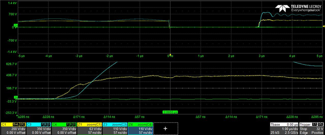
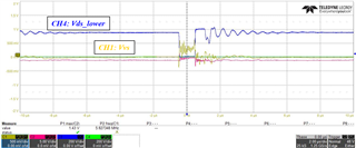
  3. Nomarl operating condition, measuring upper switch Vgs by diffirential probe, test graph is Figure 5. There it looks like already turn on.because when lower swtich turn off, upper switch Vgs is 5~6V. i wonder it is measuring mistake or not. And I expected the Vgs to rise up to 12 V due to the parallel Zener diode being rated at 12 V. However, it only reaches 7-8 V. (Of course, I also confirmed in the guide document that the Vgs only reaches 7-8 V.)

  4. Given the ringing on the lower FET and the observations from points 2 and 3, could it be that the upper FET is always turned on?

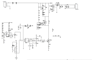
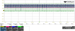
Fig.1 (CH1: D13 V, CH2: Vout, CH3: lower FET Vds, CH4: lower FET Vgs // Vin: 500Vdc)
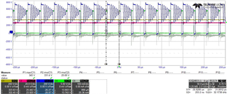
Fig.2 

(CH1: D13 V, CH2: Vout, CH3: lower FET Vds, CH4: lower FET Vgs // Vin: 500Vdc)

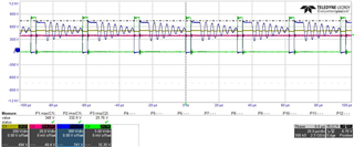
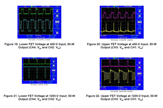
Fig.3 (CH1: D13 V, CH2: Vout, CH3: lower FET Vds, CH4: lower FET Vgs // Vin: 500Vdc)

Fig.4 CH1: D13 V, CH2: Vout, CH3: lower FET Vds, CH4: upper FET Vgs // Vin: 290 Vdc)

Fig.5 CH1: D13 V, CH2: Vout, CH3: lower FET Vds, CH4: upper FET Vgs // Vin: 290 Vdc).

when nomal condition, lower swtich Vds is below. sometime it dosen't have ringing and sometime have. I wonder it is why.

  • Hi Seungpyo,

    Thank you for reaching out.

    Firstly, regarding the cascode flyback please refer the following article which might be helpful.

    https://www.ti.com/document-viewer/lit/html/SSZTBZ61.

    Are you referring to the DCM ring? I think this will depend upon the loading and choice Lm for the application which eventually decides the switching frequency.. A higher Lm will push Fsw lower and probably there is going to be DCM ringing which will be seen. So this should be ok.

    2. For probing the upper FET, we would recommend using differential probes.  What you are observing is some coupling through th probe which probably interferes with the Vs pin sensing and makes it start at lower input voltages.

    3 & 4. Please refer this app note

    https://www.ti.com/lit/ta/ssztbz6/ssztbz6.pdf?ts=1725644086569&ref_url=https%253A%252F%252Fwww.google.com%252F#:~:text=It%20is%20important%20to%20have,capacitor%20in%20parallel%20with%20ZC.

    regards,

    Harish

  • Thank you for your response. However, there are still a few unresolved points.

    These are questions regarding points 3 and 4.

    When Vin is greater than Vzc, I understand the process as follows

    1) Cc charges, 2) when the lower switch turns on, 3) Cc charges Cg, and 4) S2 turns on.  

    5) When turning off S1 turns off, 6) Cg's energy moves back to Cc, and 7) the upper switch turns off.

    However, I don't understand why the Vgs of the upper switch still measures a voltage even when the lower switch turns off. As can be seen in the graph, approximately 5V is measured (using a differential probe). Please refer to the attached graph.

    (CH2: Vgs_upper swtich, CH3: Vds_lower swtich, CH4:Vgs_upper swtich @Vdc_input :600 V)

    In the attached document, the discharge process explains that Cg's energy moves to Cc, and therefore, no voltage should be measured on Cg.

    Moreover, considering that the Vgs(th) of the STD2N95K5 MOSFET is Min. 3V, I am concerned that the measured voltage could already turn on the upper switch.

    Thus, I am curious if this voltage behavior is typical when following TI's reference design.

  • Hi Seungpyo,

    How is the upper MOSFET gate voltage measured? Just make sure there is not any offset in the measured voltage using differential probe.

    Ideally as the lower FET turns off, the voltage across the source of the upper FET should build up and Vgs there should fall below the threshold. The charge probably Cg is not shunted into Cc. Please check the clamping of Vz2 across the gate of upper FET. This could be clamping this nde.

    Regards,

    Harish

  • Hello! I have conducted the experiment as follows, reflecting your feedback.

    After careful consideration, I would like to ask additional questions. I understand you must be busy, but I would appreciate it if you could review them.

    First, I measured the voltage of the suggested Zener diode and the Vds of each switch.

    • The following waveforms are from an experiment with a 550 Vdc input.
    • CH1: Lower FET Vds, CH3: Upper FET Vds, CH4: Vzener_gate_upper
    • Issue 1: When Vin > Vzc (Vin: 550Vdc > Vzn: about 678V), the Upper FET does not experience Vds. However, in my case, there are times when Vds is randomly applied, and other times when it is not. The Vds of both FETs is measured irregularly during turn-off.
    • Issue 2: Regarding this issue, I analyzed the turn-off times of the Low FET and the Upper FET.
    • My opinion: In my experimental waveforms, the difference in Vds between the Low FET and the Upper FET is less than 50ns.
    • My Conclusion: Therefore, it operates as if Vin > Vzc, but because the turn-off times of S1 and S2 do not differ significantly (>50ns), I believe the operation is random.
    • suspected Cause: Although I used the PCB artwork recommended on TI’s website, I suspect that the gate driver circuit might have a slightly longer PCB trace, resulting in parasitic inductance.
    • My Potential Solution: I am considering lowering the gate driver resistance or adding a turn-off diode as potential solutions.

  • Hi Seungpyo,

    Sorry I was not able to respond quick as there were other things going on.

    I think your analysis is correct. Some significant difference in turn off delay can result in the upper FET experiencing this random Vds behaviour.

    I think in addition to optimizing the lower FET turn off, upper switch Vds showing up will lot depend on how quickly the clamping on the low side FET occurs. Which means the top FET's zener connected across its gate and capacitance on gate should discharge quickly minimizing this turn off delay in upper FET. You can refer to this report where switch node is plotted wrt low side switch drain voltage. I think this should depend a lot on the ringing at switch node and the turn off times of the two FETs.

    https://www.ti.com/lit/ug/tidt266/tidt266.pdf?ts=1726197429537

    Regards,

    Harish 

  • Thank you for your response despite being busy. However, I have a few questions.

    1. I am conducting experiments with an input voltage of 650V.

    2. I have changed the gate capacitance of the Upper MOSFET from 4800pF to 3200pF, and also adjusted the gate resistance to 8 ohms.\

    3. As a result, I was able to achieve stable turn-on and turn-off behavior

                                                                                                  (CH3: Lower fet, CH1: Upper fet, @650Vdc)

                                                                                                (CH3: Lower fet, CH1: Upper fet, @1000Vdc)

    4. However, contrary to the guidance you provided, I am still observing voltage on the Upper MOSFET's Vds even when Vin > Vzc.

    5. I would like to understand the reason for this.

    6. My opinion is that while Vin > Vz, the sum of Vin + N*vout + Vspike exceeds Vzc. Therefore, it clamps at Vzc and the remaining voltage is applied to the Upper MOSFET.

    I would appreciate your response regarding my analysis.

  • Hello,

    Thanks to your support, I have successfully completed the experiment using the SMPS made with the PCB reference provided by TI.

    But, I made copy version of reference, I have designed the circuit as per the document number, using the same components. However, the PCB layout is designed differently.

    However, the SMPS with the PCB that I designed is not working. I have identified the following issues. Please feel free to share your opinion if you think the issue is caused by something other than what I have identified

    1. During the initial 3-pulse operation, the voltage applied to the shunt resistor is too high. At this moment Vin is 350 Vdc. Normal operating PCB SMPS case, the value of this about under the 300mV. But in my case, about over the 500 mV. If Vin is more than 350Vdc, the PWM IC of initial 3 pulse is stop.   
    2. NTC pin signal is correct. So i guess CS or VS pin have problem.
    3. At the Shunt R, Initially, I used a 0.9-ohm resistor, but due to the high shunt voltage, I replaced it. Currently, a 0.3-ohm resistor is installed. The below waveform is 0.3-ohm condtion.
    4. The voltage on the CS pin is also high, so I modified the values to R: 0.9k and C: 200pF. The below waveform is R: 0.9k and C: 200pF.
    5. Despite these changes, the shunt voltage is still 500 mV during the 3-pulse operation, even in a no-load and non-operational state.
    6. The transformer and MOSFET are the same components as those used in the reference. only PCB patten is different. 

      I wonder your opinion and How can I operating this PCB board?

    Please review the waveforms below.

  • Hi Seungpyo

    Thank you for reaching out.

    The voltage applied to the CS pin resistor should be close to Vcs(min) value during the 3 exploratory pulses during startup. 500mV definitely seems on the higher side. Have you tried replacing the IC to see if any issue is here? This is peak current controlled and follows the control law. So it might be possible that despite changing the sense resistor there is no difference here. Also the Vs signal looks very distorted which will also have an effect.

    Please let us know your observations.

    Regards,

    Harish

  • After receiving the following comments, I replaced the PWM IC, but the issue remains the same.

    I believe this is due to the effect of the PCB layout. I laid out a wide ground plane for the components in the red box indicated in the schematic. Additionally, for the shunt resistor, I connected it to the ground in a bus configuration.

    All other passive components, as well as the transformer and MOSFET, are the same. However, I can't help but think that these abnormal behaviors are due to the effects of the PCB routing.

    If you have any other opinions or comments, please feel free to share them. Thank you.

  • Hi Seungpyo

    Thank you for the reply.

    I think the GND for controller signals looks very long. Ideally there should be a big pour to the controller signal GNDs from negative of C1. The gate return looks very long and this needs to be checked. The boxes which you show needs to be wide as suggested but all these needs to be a continuous big pour region to be effective.

    Regards,

    Harish