This thread has been locked.
If you have a related question, please click the "Ask a related question" button in the top right corner. The newly created question will be automatically linked to this question.
Tool/software:
hello. My name is Myungsu Kim.
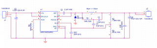
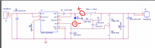
A DC-DC converter circuit was designed using LM5013, using the design tool provided by TI.
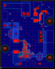
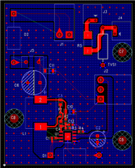
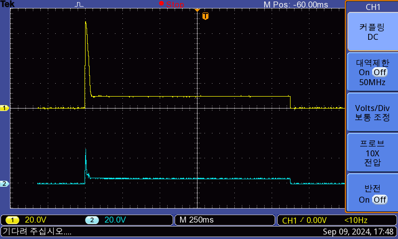
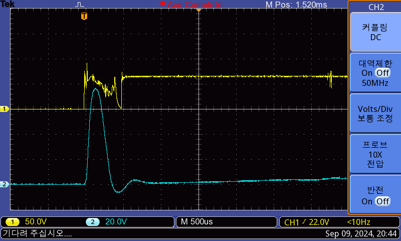
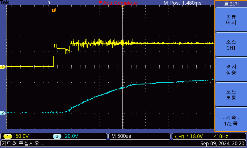
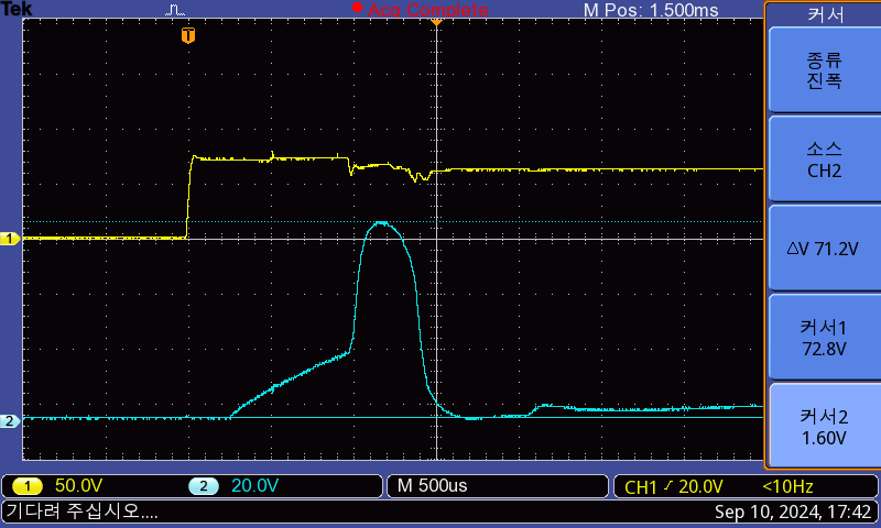
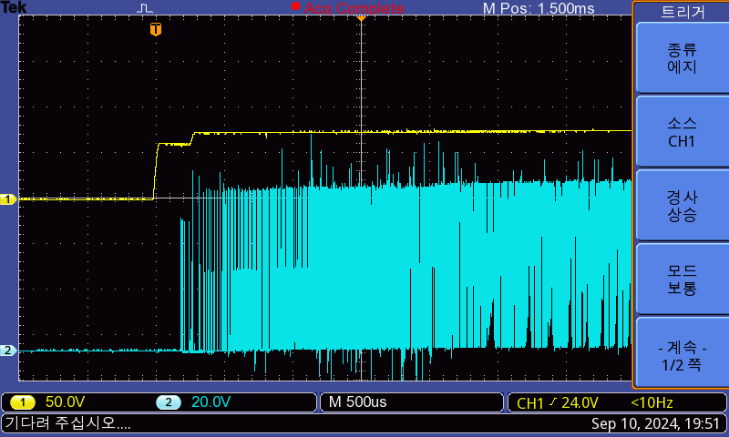
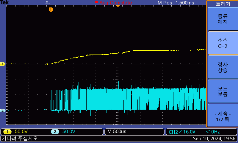
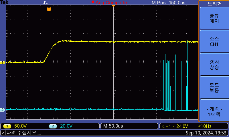
The PCB was designed and the components were assembled as samples, and during testing, the LM5013 CHIP was destroyed while applying input voltage to two samples.
One CHIP exploded and one caught fire.
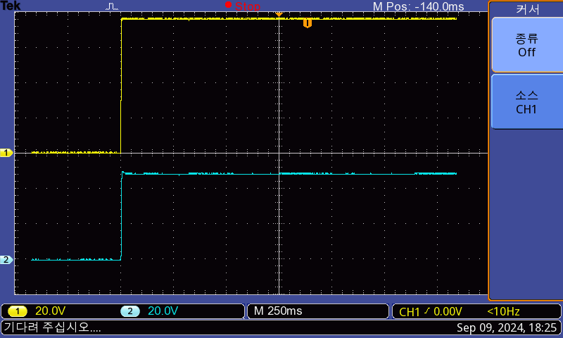
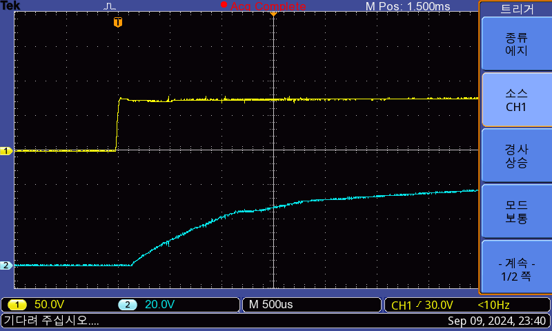
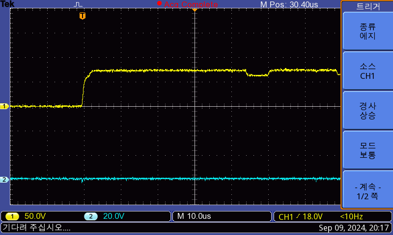
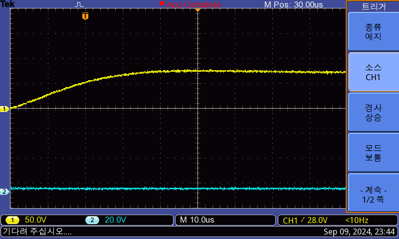
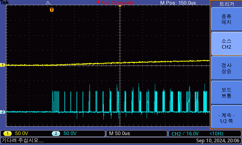
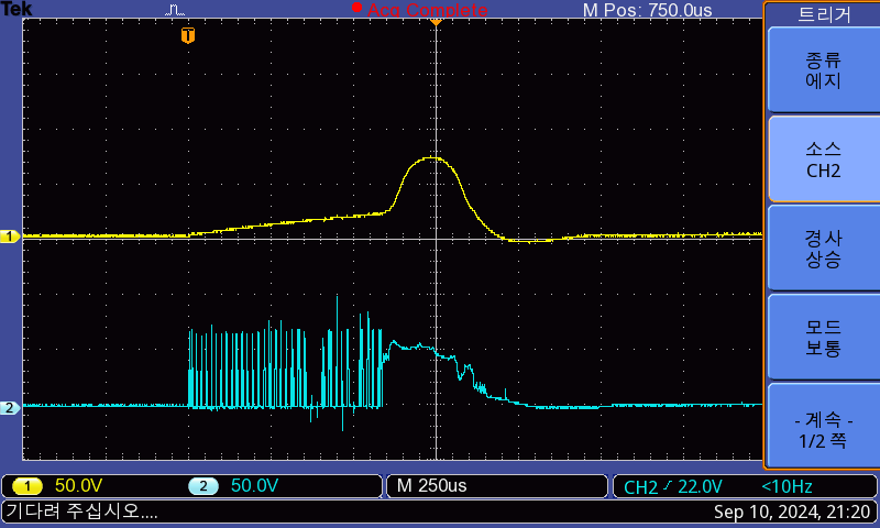
The input/output conditions are,
The input voltage was set to DC76V and the output voltage was DC48V, and the input voltage was supplied by connecting the battery.
The input voltage was supplied using a connector, but it is not clear whether the + voltage was connected first and the - voltage was connected later.
I don't know if this was the cause, but I would like to know what problem could cause this phenomenon.
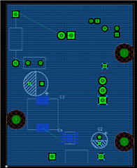
I am uploading the circuit diagram and CAD data attached.
Please review


In both samples in question, destruction occurred near pins 2 and 3 of the LM5013 CHIP. After that, a short occurred between PIN 1 and PIN 2 and 3.
Hi Kim,
The issue could be due to input voltage transient during hot plugin. Can you please measure the input voltage across the input capacitor C2 , switch node and output capacitor during start up?
Thanks,
Nitya
Hi Nitya,
I don't understand exactly what you mean. Can you explain it easily?
Which part do you want to measure based on the reference number?
Thanks,
Kim
The + side of C2 is a yellow waveform, and the + side of C6 is light blue.
The first picture is when the output is normal, and the lower picture is when the LM5013 CHIP is destroyed.


Hi Kim,
In failed case, the input voltage is within the abs. max limit as per above waveform. This could be due to sampling limitation of the oscilloscope as well. I would like you to do couple of experiments.
1. With existing schematic and layout, capture the input voltage (C2 capacitor) and GND with 10usec/20usec/100usec time scale.
2. It is recommended to use the electrolytic capacitor at the input of the LM5013 if there is lengthy cable from battery to input of the device to dampen the LC oscillation. Try soldering 33uF/47uF electrolytic capacitor in parallel to C2 capacitor.
Thanks,
Nitya
Hi Nitya,
I changed the C2 value from 2.2uF to 47uF and measured it.
We were able to obtain much more stable values.
In the attached picture, the first picture is with C2 set to 0.1uF,
the second picture is with 2.2uF, and the third picture is with 47uF.
The first picture shows C2 set to 2.2uF and the second picture shows C2 set to 47uF.
In my opinion, there will be no problem if you select C2 as 47uF.
Hi Kim,
Good to know that issue is resolved by changing the input capacitor values. It is always recommended to place the electrolytic capacitor at the input of the device to dampen the LC oscillations.
Thanks,
Nitya
Hi Nitya,
I made several samples and tested them by replacing C2 with 47uF. However,
in two samples, PINs 2 and 3 of the LM5013 CHIP are broken as before, causing GROUND PIN and SHORT.
I am attaching the photo captured at this time. Please review
The yellow waveform is the input voltage DC75V, and the light blue waveform is the output voltage 48V,
but when a fault occurs, the highest value in the picture instantly rises to 72V.
Hi Kim,
This is strange. The input voltage is pretty much stable. However the output voltage is soft starting as expected for some 700usec and suddenly the output voltage overshoot is observed causing the output voltage to reach around 70V. Can you measure the switch node waveform as well along with input voltage and output voltage to debug further?
BTW, on how many boards you are seeing this issue and what is failure rate?
Thanks,
Nitya
Hi Nitya,
Which part of the switch node waveform are you talking about?
Can you tell me the exact location?
Four sample test quantities and defective quantities were tested, and two of them had the same defect.
Hi Kim,
Refer below image marked in red. This is the location of switch node of dc-dc converter.
The input power supply method is first connected to the test sample using a cable with a 2-contact mechanical switch connected
in the middle of the POWER SUPPLY, and then turning the switch ON/OFF to supply power to the test sample.
Among the attached pictures, numbers 1 and 2 are the input voltage and measured values of the switch node,
and numbers 3 and 4 are the output voltage and measured values of the switch node.
These pictures are the measurement waveforms of the sample that was not destroyed among the four samples.
When supplying input voltage to a test sample, a picture of when the sample fails is captured and attached.
The yellow waveform is the output voltage, and the light blue is the switch node waveform.
Following up in "https://e2e.ti.com/support/power-management-group/power-management/f/power-management-forum/1411792/lm5013-i-have-a-question-regarding-lm5013-please-review" thread.