This thread has been locked.

If you have a related question, please click the "Ask a related question" button in the top right corner. The newly created question will be automatically linked to this question.

TPS2HB35-Q1: Be damaged or degeneration when there is negative bias offset on Gate and Source

Part Number: TPS2HB35-Q1

Tool/software:

Hi Team,

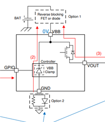
Customer would like to confirm if the device will be damaged or degeneration when there is negative bias offset on Gate and Source.

For example, when the input voltage is 0V, there is open circuit detection on output port or short to battery, it may cause the MOSFET turned on due to energy transfer.

Thanks

Best,

Frank

  • Hello Frank, 

    To add protections against scenarios like short to battery it is best to implement a reverse blocking diode on the VBB pin. In addition, implementing a GND network (a diode in parallel with a resistor on GND pin) will protect the device in this application. I added a snip from Figure 39 in the datasheet to display this design. 

    Best Regards,

    Alan

  • Hi Alan,

    Customer cannot modify the layout anymore. Could you please comment if without any reverse diodes and resistors, would it be risk?

    Thanks

    Best,

    Frank

  • Hello Frank, 

    Without any protections from reverse battery the device may sustain damage. In the reverse battery condition, the switch will automatically be enabled regardless of the state of EN1/EN2 to prevent excess power dissipation inside the MOSFET body diode. In many applications (for example, resistive loads), the full load current may be present during reverse battery. In order to activate the automatic switch on feature, the SEL2 pin must have a path to module ground.

    Best, 

    Alan