This thread has been locked.
If you have a related question, please click the "Ask a related question" button in the top right corner. The newly created question will be automatically linked to this question.
Tool/software:
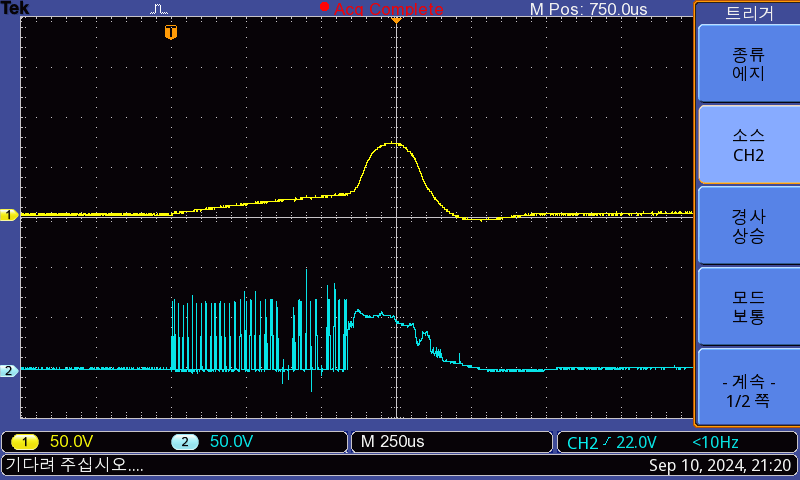
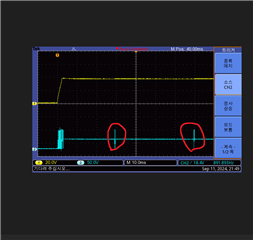
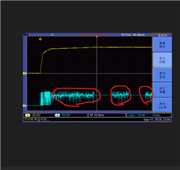
I am posting the question again because the issue related to LM5013 has not been resolved. Please review
Hi Nitya,
I would like to ask a question again because the problem I posted earlier was not resolved.
We capture and attach the measurement waveform for the sample that failed during testing.
When supplying input voltage to a test sample, a picture of when the sample fails is captured and attached.
The yellow waveform is the output voltage, and the light blue is the switch node waveform.
Hi Kim,
Checking internally about this. Will get back to you in couple of days.
Thanks,
Nitya
Hi Kim,
Couple of things i would like to highlight to debug further.
1. Recommend you to put ABA swap test for the device. Meaning solder good LM5013 device [already tested] to bad board and check the device behavior. In this way we get to know if there is any issue with existing board.
2. I looked into your schematic and layout. In schematic, It is recommended to keep ceramic capacitor at the input along with electrolytic capacitor. The ceramic capacitor needs to be as close as possible to device.
3. The ripple generation uses type-3 ripple generation methods. This is more suited for ceramic capacitor at the output side. But in this design, the output capacitor is electrolytic. Recommend you to use the ceramic capacitor at the output.
4. The feedback resistor R2 is higher than 1Mohms. TI does not recommend a RFB1(R2) larger than 1 MΩ as the feedback path becomes more susceptible to noise. Ensure to route the feedback trace away from the noisy area of the PCB, minimize the feedback node size, and keep the feedback resistors close to the FB pin.
Thanks,
Nitya
Hi
I tested it as you advised. I need to do more tests.
The problem of LM5013 CHIP being destroyed seems to have disappeared.
I have some questions during the test, so I would like to ask you some questions.
Let me ask you a question while looking at the following picture.
The yellow waveform in the picture is the output voltage, and the light blue waveform is the switch node waveform.
In the first picture, the output voltage was measured by adjusting the FB value to about 34V, and in the second picture,
it was measured by adjusting the FB value to about 54V. I would like to know if the part marked with a red circle in the picture
is normal, especially the part marked with a red circle in the second picture. The waveform is not clean and looks like noise.
What is the cause?
Hi Kim,
This is due to oscilloscope sampling issue. This is expected if the time scale is large on the oscilloscope.
This is not related to device behavior.
Thanks,
Nitya
Hi Kim,
If no further query on this issue, i recommend you to hit "resolved" button.
Thanks,
Nitya