Because of the Thanksgiving holiday in the U.S., TI E2E™ design support forum responses may be delayed from November 25 through December 2. Thank you for your patience.

This thread has been locked.

If you have a related question, please click the "Ask a related question" button in the top right corner. The newly created question will be automatically linked to this question.

UCC28064A: Parallel two devices - confusing external devices as per SLUAAD0

Part Number: UCC28064A

Tool/software:

Hi, I'm looking at the SLUAAD0 application note on how to parallel two UCC28064A PFC controllers.  I'm really confused by this part of the document...
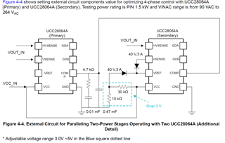
The note implies we can adjust the resistive divider in the blue square to get between 3 and 5V from VCC - but what does this do?  The other end of the diode is VREF, which is 6V, so will be reverse biased at all those voltage levels and so I can't work out what we're doing here.

  • Hello Tom, 

    I agree that this part of the document is confusing.  After some study I think I figured out the problem and how to resolve it. 
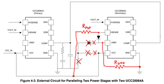
    Figure 4-2 of the App-note makes sense, and we'll use that as the basis for analysis and design.  I think Figure 4-4 is "miswired". 

    To get the secondary controller to operate but to not fight the primary controller, it is necessary to make the secondary VSENSE (call it "VSENSE2") to fall within certain tight constraints. 

    First (based on UCC28064A Fault Logic Diagram Figure 30) , VSENSE2 must be > 1.25V simply to Enable the IC to operate. 
    Next, VSENSE2 must be > 3V to disable the High-Gain mode of the Error Amplifier before start-up.
    Next, VSENSE2 must be > 5.9V to disable the High-Gain mode of the Error Amplifier after start-up.
    Next, VSENSE2 must be > 6.00V to force the Error Amplifier to sink current, but not too much current, so not too much > 6.00V.
    Finally, VSENSE2 must be < 6.36V to ensure that the OV-Clear signal can be true to always reset the Low_OV Latch in the event that spurious noise somehow briefly raises VSENSE2 above the 6.48V LOW_OV fault threshold setting the Latch. 

    I believe that is the reason the VSENSE2 diode to VREF is shown as 40V, 3A, which can be assumed to be a sizable Schottky diode such as MBRS340 or equivalent. 
    The intention is that the actual diode current will be <1mA, and hence the diode forward voltage drop should be quite small. 
    My first concern is to select a Schottky diode whose worst-case Vf is < 0.3V at the lowest ambient operating temperature expected, such as -40C.  
    (As an aside, one may assume that the bigger diode has lower Vf, but reviewing some specs, I find that some 1A diodes in smaller packages may actually have lower max Vf at -40C that the 3A diode does.  Check out MBRS120 and B120/B, for example.  Note, I think a 20V rating is sufficient and may provide lower Vf.)

    My next concern is to minimize the current being sinked (sunk?) but EA2, which will constitute an offset current (load current) on EA1 which is controlling the regulation.  
    Since the small-signal range (low-gain of 55uS) of the EA is only +/- 15uA, we don't want to load EA1 by more that a few uA. 
    1uA at 55uA/V = 18mV offset from VsenseReg.  Assuming this offset is Vf of the Schottky from VSENSE2 to VREF2, we can extrapolate the Vf curve of Onsemi MBRS140T3G Figure 2 Maximum Forward Voltage from 0.02A down several decades to estimate how much current is allowed at a certain temperature.

    Using a really crude extrapolation scale on my display screen of 1" = 1 decade, I estimate for the -40C curve that Vf = 20mV at about 6" = 6 decades below 0.2A. Each inch is 1/10, so 6" is 10^-6 of 0.2A = 0.2uA forward current.  This is an absurdly low current, so I must accept higher Vf and consequently higher offset current out of EA1, at least at the very coldest ambient temperature.  Things are much better at higher ambients.  Designers should verify actual operation at lowest temp.  

    To make a long story shorter, Rpup = (12Vcc - 6Vref) / 1uA = 6Mohm pull-up VSENSE to VCC.  Diode current scales from this calculation, as VCC varies and as the pull-up value is adjusted.  Users of this App-note can decide how much current to provide through the Schottky.  
    Note: The VREF is not a current sink, it is an internal source that provides bias power to most of the IC circuits.  The VREF pin is provided to allow connection of external bypass capacitance (for stability) and a very limited amount of output current for low-power peripheral circuits.  The internal bias currents go way down during burst mode dead times, so I suggest that a "minimum load" be applied on VREF to GND to sink the same or greater current as is supplied from VSENSE2 through the diode. Rsink = 600kR applies a 10uA load on VREF, for example, without significantly stressing or affecting VREF regulation. 

    Finally, I have modified Figure 4-4 to show how I think this circuit should be connected.  

    As an afterthought, maybe a small ceramic filter cap (~1nF maybe?) can/should also be added from VSENSE2 to GND, to provide noise filtering.
    Make sure to NOT excessively filter VSENSE1, so as not to interfere with transient response and OVP.  A time constant of ~100us would be suitable for VSENSE1.

    Regards,
    Ulrich

  • Hi Ulrich - that makes a lot more sense than what's in the app note.  Basically we want VSENSE to be higher than VREF, but by the smallest amount possible so EA2 is not pulling against EA1.  Funnily enough I had already considered a pull-up on VSENSE because I couldn't see how the diode was biased, but I then got totally thrown by the resistor divider in the note.
    I think VREF already has some load on it due to the resistor divider for the PHB pin, so I don't think the Rsink in your sketch is a necessary addition.

    With that clarified, as another question on this setup, can I tie the PHB, BRST, VINAC and HVSEN pins together between the devices, or would it be wise to allow them to have slightly shifted trigger points so that device2 can switch on/off before device1?

    Thanks, Tom

  • Hello Tom, 

    Good point about PHB divider loading VREF already.  That saves adding another part. 

    I think it would be wise to have separate settings for PHB, BRST, and VINAC for the two devices. 
    That way you can sequence them as desired.  You can make the device2 VINAC hysteresis narrower or shifted lower than device1 so that device1 always dominates start-up and shutdown in Brown-in/Brown-out situations. 
    I think HVSEN2 should be set higher than HVSEN1, so that the COMP discharge to 20mV can always be accomplished in device1 (the primary controller). 

    This arrangement is new to me, so I don't know of any subtle down-sides to the settings as I proposed above.  
    It seems like it should work okay, but don't assume that there is nothing that can go wrong.  
    Careful study of the various thresholds and sequencing can help to identify any potential issues.

    Regards,
    Ulrich

  • Actually thinking about the Vsense >Vref.  My Vcc is 14V.  Why can't I just put a 100k/120r divider between Vcc and Vref which would give me +15mV on Vsense?  No messing with a diode.

  • Hello Tom, 

    Your idea makes a lot of sense, and I found myself trying to figure out where the down-side is.  

    It can't be variation of VCC voltage, because VSENSE will always be > VREF even though (VCC-VREF) has a wider variation than VCC alone (percentage-wise).   We do want VSENSE to always minimally exceed VREF by a few mV greater than its max offset voltage at the error-amp inputs at the lowest VCC (at UVLO-off threshold).   

    It can't be the load on VREF when VCC is 0V, because VREF is also 0V. 

    But, VREF does not rise to 6V until VCC exceeds UVLO-on threshold. 
    The only issue MIGHT be if the current forced into VREF while VREF = 0V cannot be absorbed by the internal nodes biased by VREF and VREF rises to some undetermined intermediate voltage not controlled normally from within before start-up.  
    It may be possible that some unexpected, unspecified, uncontrollable state can be entered and worst-case latch up in that state... 
    But the same can happen using a 15mV diode drop, so that concern may be mitigated (assuming that a working design on which the app-note is based did not encounter such a situation).  (However, it is unknown how much validation testing was performed on such a system, over how big of a population.)

    Seems like a good idea, and I don't have a reason for not trying it.  I hope it works!

    Regards,
    Ulrich