This thread has been locked.

If you have a related question, please click the "Ask a related question" button in the top right corner. The newly created question will be automatically linked to this question.

TPS6593-Q1: Asking for Schematic Review

Part Number: TPS6593-Q1
Other Parts Discussed in Thread: AM62A74

Tool/software:

Hello,

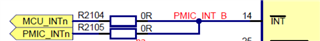
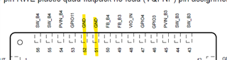
can you please provide help on review for PMIC schematic? It shall be used with a AM62A74 SoC.

I have additional questions regarding the hardware configuration.
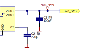
As we use three-phase configuration:

  1. FB_B3 can be used for voltage monitoring?
  2. Can it be left floating?
  3. How is it configured?

Thank you very much in advance.

Greetings Daniel

Edit: added the completed checklist

TPS65931211-Q1_Schematic_PCB Checklist_1p4.zip

  • Hi Daniel,

    Thanks for posting. As a first step, please go through and fill out the schematic checklist attached, then upload it as well as any changes: https://www.ti.com/lit/zip/slvc804

    Regards,

    Katie

  • Hi Katie,

    Thank you for your help. I've added the completed checklist to the opening post.

  • Hello Daniel,

    My comments/concerns are as follows:

    PIN49: To answer your question about FB_B3, it does indeed need to be connected to a voltage source, it is recommended to connect to the TPS22965N as shown below

    PIN14: nINT is an open drain pin, needs a pull up as noted in the checklist you provided, just making sure it's been brought to your attention.

    PIN 51 & PIN 52: Please be sure to ground these as per the recommendation of the datasheet, I see that the checklist has these listed different functionality please ignore those line items. When GND please do route them to the thermal pad, try to connect to a solid ground plane if possible.

    PIN 5 & 6: Please try to route these to a solid ground plane as well. DO NOT route these to the thermal pad.

    PIN 46: GPIO3 if the IO + DDR retention is not an option you care for this does not need to be implemented.

    PIN 23: GPIO5 is the selection for the voltage for the SD card since it is optional and not being used this can be ignored.

    PIN24: GPIO6 selection of voltage as pulled up, will be 0V85 on VDD_CORE 

    PIN 41: GPIO8 Watchdog will be disabled by default with PU resistor populated as stated in the checklist.

    PIN19: GPIO9 is edge triggered, net will have to drive this after power up has occurred for LDO2 functionality.

    PIN 42: GPIO10 is grounded BUCK4 voltage will be set to 1V1

    PIN 53: GPIO11 is left floating, SD card not used, okay to do

    Best Regards,

    Nicholas McNamara