This thread has been locked.

If you have a related question, please click the "Ask a related question" button in the top right corner. The newly created question will be automatically linked to this question.

LM5155: Thermal Shutdown/ MOSFET and diode heating issue

Part Number: LM5155


Tool/software:

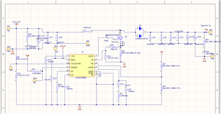
LM5155 Boost Converter Design:-

Hi ,

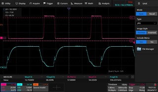
I am facing heating issue of MOSFET and Schottky Diode at below mentioned I/P ,O/P parameters.

Output getting decreased after MOSFET is heating above 120 deg.

Is it thermal shutdown of LM5155 Controller? oR Mosfet? or Inductor?

Is there any other References/parameter causing heating issue???

Vin:- 8.4V to 12.6V

Vout :- 54V/ 2A

Switching Frequency:- Fsw:- 445Khz.

Inductor is 10uH/10Amp

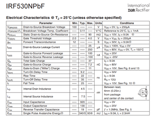
MOsfet :- IRFB4110 100V/180A

Reference Sch:-

  • Hi Chandrakant,

    Thanks for reaching out.

    Can you please send some scopeshots? I would dlike to see Vin, Vout, switchnode and COMP pin.

    I would recommend to add a slope compensatin resistor at the current sense pin, as the duty cycle for you application is very high. You can take a 1k resistor.

    Also the current rating of your inductor is too low. I would recommend to use an inductor with less inductance and more current rating.

    Did you check the design already with our quickstart calculator https://www.ti.com/tool/download/SNVC224

    or the power stage designer? https://www.ti.com/tool/POWERSTAGE-DESIGNER#downloads

    Best regards

    Moritz

  • Hello Moritz,

    Thank you for suggestion.

    I have attached Drain-Source and Gate to Source W/F for your reference along with Thermal images of the board.

    It is observed that LM5155 heating above 140 degree @ 0.6A laod @ 54V Vout.

    Mosfet is also heating above 100 degree.

  • Hello Chandrakant,

    I see the FET is turning on very slowly. This will cause a lot of heat. Are you sure the resistor R27 is 0 Ohms?

    Where is the supply for the IC (SW on) coming from?:

    Can you try to connect this directly to the 12V input please?

    Does Vout in this case even reach 54V? Can you please send a scopeshot showing Vin, Vout , Switchnode and CS pin?

    Because the dutycycle should be much higher. So the current limit might also be hit.

    Best regards

    Moritz

  • Hello Moritz,

    Thanks for quick response.

    Yes Gate resistance is Zero Ohm.

    As you suggested I am using 1k for slope compensation.

    Yes FET is turning on slowly.. I have checked its Vth is min 2V and Rds ON is 4.5mOhm.

    In my design BIAS AND VCC are directly connected to the Vin. that is 12.6V max.

    I am getting max Vout as 53.24V.

    Duty cycle is 86%.. Its gradually increasing from 70% to 86% with respect to increase in Iout. 

    • LM5155 IC got burn twice while testing.

  • Hi Chandrakant,

    As you suggested I am using 1k for slope compensation.

    With adding this slope resistor, it might be neccessary to decrease the current sense resistor. Please use the quickstart calculator to calculate a proper value.

    In my design BIAS AND VCC are directly connected to the Vin. that is 12.6V max.

    Ok, can you please send an updated schematic then? Did you already try to disconnect VCC from Vin?

    Duty cycle is 86%.. Its gradually increasing from 70% to 86% with respect to increase in Iout.

    You are right, i am sorry, i mixed up the 2 waveforms, as the red one is labeled as VGS.

    Did you already change your inductor? The current rating is not sufficient. Also the inductance value can be lower.

    Please send me a scopeshot that shows the following signals in one picture as requested above:

    Vin, Vout, switchnode(Drain of the FET) and CS.

    Best regards

    Moritz

  • Hi Moritz,

    I have using Mosfet  IRF530NPbF with lesser Qg.

    I am getting good Gate pulse at internally regulated VCC.

    Drain is not Getting turned off properly upto 0.5A of Iout.

    Once load increased above 0.6A I am getting proper Drain pulse(please refer attached Waveform).

    L=10uh/10A.

    Slope compensation resistor Rsl=1Kohm

    Rsense :- 5mOHM

    COMP circuit:-

    Rcomp : 2.2kohm

    Ccomp: 22nf

    Chf :- 220pf

    Fsw:- 170Khz.

    With above values Mosfet is heating less as compared to before.

    LM5155 not heating but INDUCTOR L temperature rising above 90 degree @ 0.8A or 1A load.

    Please check attached Waveform and thermal images for your reference.

  • Hi Chandrakant,

    Thanks for your reply.
    Moritz is out of office today, so please expect a response by beginning of next week.

    Thank you very much for your patience.
    Best regards,
    Niklas

  • Hi Chandrakant,

    As mentioned in the previous posts, the current rating of the inductor is not sufficient. This is the reason for the heat.

    Please change your inductor.

    Please use an inductor with a higher current rating and less inductance. You can use the quickstart calculator or the power stage designer to find a proper value.

    Also i recommend to use more input capacitance, as i can see a ripple on the input voltage.

    Best regards

    Moritz

  • Hi Moritz,

    I have change the Inductor with higher current rating 18A/20A I saturation current and Mosfet to SMD package (BSC0802LSATMA1).

    I am not able load it above 15W of output power.

    Vin:- 8.4V to 12.6V

    Vout :- 54V/ 1.5A

    Switching Frequency:- Fsw:- 445Khz.

    Inductor is 8.2/18Amp

    MOsfet :- (BSC0802LSATMA1).

    Before i was using Through whole mosfet and i was able to draw current upto 1.6A , after doing changes with layout , Inductance and Mosfet I am not able to get the desired Output Power.

    I am following LM5155 quick start design calculator and Webench power designer but not getting proper outcomes.

    Please check attached waveform for reference.

  • Hi Chandrakant,

    Can you send me the datasheet of your inductor please?

    What waveforms did you share? I think it is gate and switchnode right?
    Normally, the dutycycle for your application should be much higher. At 12V Vin around 77%.
    You might hit the peak current limit. You can check the voltage at the CS pin.

    Best regards

    Moritz

  • Hi Moritz,

    I have attached Quickstart design which i am following for my design.

    As you can see in attached images that the Drain peak to peak voltage reaching above 90V @0.4A due to which MOSFET and Inductor is heating and Iam not able to achieve desired output current.

    I am using 3.3uH Inductor 18A current and 30A of Saturation current (SRP1265A-3R3M) and Mosfet 20A/156A 100V (BSC034N10LS5ATMA1) with low Rds ON 3.4mOHM and low Qg. and Diode (SS2PH10-M3/84A) 2 in parallel.

    Soft start, Compensation loop , FB loop and Current Sense values are as per quickstart design.

    Please suggest why mosfet Inductor diode are heating @ very less load current???

    Is there will be any issue with PCB Layout.(All the components are SMD) for MOSFET DRAIN Spike and Gate ringing when Turned OFF??

    Please go through the Waveform and suggest if any change needed.

    Thank you very much for your support....

    3386.Copy of LM5155_56_Quickstart_Calculator_for_Boost_Converter_Design_V1_1_1.xlsx

  • Hi Chandrakant,

    First please add some gate resistance (2-5 Ohms) and add snubbers across the diode and the FET. This should reduce the ringing.

    Then you can try again. https://www.omicron-lab.com/fileadmin/assets/Training_and_Events/Power_Analysis_and_Design-Symposium/2022/Presentation_BirichaDigital.pdf

    You can also send me your layout files to check.

    Best regards

    Moritz

  • Hi Moritz,

    Thank You ....

    Let me try with the above mentioned suggestions.

    I will get back to you once checked all the possible causes....

    Thank You.

  • Hi Moritz,

    Please check attached file,

    There difference in Compensation circuit in WEBENCH, datasheet and Evaluation board.

    Evaluation board has C24 before R17 but in actual board image in the Evaluation board documents showing Resistor is soldered on the place of C24 and capacitor on R17.

    Please guide me with the comp loop components placements.

    Does it will cause Spikes in Drian to Source Voltage pulse.

    Thank You...

  • Hi Chandrakant,

    The order of these two parts does not matter.

    Also it will not cause spikes. You can damp the spikes by using snubbers.

    Best regards

    Moritz