This thread has been locked.

If you have a related question, please click the "Ask a related question" button in the top right corner. The newly created question will be automatically linked to this question.

UCC21732: Full Bridge Inverter

Part Number: UCC21732

Tool/software:

Hello Experts,

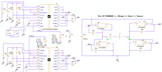
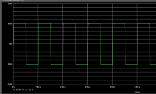
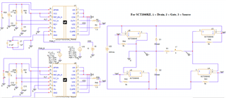
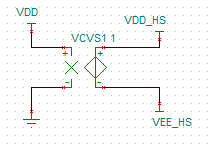
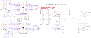
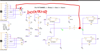
I have the following full bridge circuit with UCC21732 gate driver and SCT2080KE SiC Mosfet. I gave 400Vdc, but I did not get its equivalent at the output side (I got 10V only). I did not understand where the problem is. Could you please help me to fix this Full Bridge Inverter circuit?


Kindly provide insights on the above points

Best
Biruk


  • Hi Biruk,

    It seems like your high-side supply is not isolated from the low-side. You will need either a "bootstrap" diode circuit, or a separate power supply that is referenced to the switch node, not ground, so the gate driver can output 10V above the switch node at all times, which is required to hold the high-side FET ON.

    Best regards,

    Sean

  • I also noted that Gate is tied to source with 5 ohms, You need to increase the Gate to source resistance to be in Kohms.

  • Hello Guys,

    I am not sure if I did exactly what you suggest; I just got the same result again without the diode. When I use the diode, it does not converge. Can you skech your suggestion on the uploaded schematic? And I'm using PSpice for TI. 


  • Hi Biruk,

    You can't use real diodes in PSPICE for convergence reasons. You can use a voltage controlled switch that will emulate a diode instead:

    Even so, your diode placement does not create a bootstrap circuit. Your VDD net is tied to both the high-side gate driver and the low-side gate driver supplies, and your ground is also tied to both gate drivers. That is the problem. You should use a second voltage source to power the high-side. Here is a suggestion:

    This will allow the voltages that supply the high-side gate driver to float on top of the switch node, as it rises when the high-side switch is turned on.

    Best regards,

    Sean

  • Hi Sean,

    Hi everyone,

    I’m still confused and would like to use the bootstrap circuit attached below for a Fullbridge configuration, but I’m not getting the expected results. Could you please provide your comments, examples, or any reference designs to help me out?

    Thanks in advance!


  • Hi Biruk,

    Are you trying to drive both a high-side and a low side FET with Vgs2? This will not work. The source voltage of U3 will rise up to 15V, and even though Vgs2=15V, the Vgs across U3 will be 0V and the switch will not be closed. You will need another channel for this high-side FET.

    Also, for this high-side supply you will need to untether your COM_1 from ground. COM_1 needs to be able to float to the source voltage of the driven FET.

    Best regards,

    Sean 

  • Hi Sean,

    Did you mean that I'll need four UCC21732 gate drivers to drive the full-bridge circuit? As I understand from your suggestion, UCC21732 can drive either the high-side or low-side MOSFET, so I would need to use two UCC21732 gate drivers to control two MOSFETs in one leg (one for the high-side and one for the low-side).

    I was trying to use one gate driver for one leg (one high-side and one low-side MOSFET) and another gate driver for the second leg (one high-side and one low-side MOSFET). But  I realized that UCC21732 is a single channel gate driver, meaning it can drive one MOSFET (either high-side or low-side) at a time, right, Sean?.  Or may I use parallelly, to reduce the required UCC21732 gate drivers ?

  • You will need at least 3. Since U4 and U6 both have their source =Ground, you might be able to combine them. U3 and U5 each need their own gate driver.

    -Sean

  • Okay Sean, I will try that.

    To reduce the gate driver requirement, what if I can use the gate driver in parallel?

    ~ Biruk

  • I do not know how your power supply control works, but you need a separate power supply for the high-side gate driver and the low-side gate driver. They cannot be in parallel.