This thread has been locked.

If you have a related question, please click the "Ask a related question" button in the top right corner. The newly created question will be automatically linked to this question.

TLC6C5748-Q1: Source Code Example

Part Number: TLC6C5748-Q1

Tool/software:

Hello,

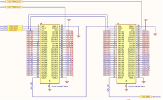
 I have been working from the data sheet to create a driver for the TLC6C5748, but the behavior I am seeing does not match what I would expect.

Could I please see your source code example so I can compare and see what I might be doing wrong?

Thank you so much,

-Scott

  • Hi Scott, 

    Do you need C code? The samle code is based on msp432p4111.

    I will share it later.

    BR, Gracie

  • Hi Scott,

    Do you capture your SCLK, SIN and SOUT waveform?

    BR, Gracie

  • Hello Gracie,
     I was able to fix most of my problem. There were some SPI settings that needed to be updated.
     I am however still having one main problem that I hope you can answer:
    I have 2 TLC6C5748-q1 chips in series as you can see in this schematic:
    The problem I am having is that I can not get the second controller to do anything.
    It is not entirely clear from the document: TLC6C5748-Q1 16-Bit Data Format Example (ti.com)  what the correct format is for the commands when talking to 2 chips.
    I have tried just about every format combination I can think of for the first command that contains the DC/MC/BC/FC values. 
    Can you please tell me, should the message have simply 15 bits in the front, then a total of 769 trailing bits, or should it then have another group of those 769 bits repeated?
    Should there be a latch between these? It is so very unclear al the documentation I have seen.
    I need to make sure that I am sending the correct format so that I can conclude that there could be a h/w problem with the board.
    Any help you can give me would be greatly appreciated!
    thanks,
    -Scott
  • Hi Scott,

    What's the application of this one? I notice you use 2 different clock sources for the GSCLK. If these 2 LED drivers use the same PWM frequency, then it's unnecessary.

    For the daisy-chain read and write, pls refer to the slides:

    2308.TLC6C5748-Q1 program procedure.pptx

    You need to write 769bits *2 and then latch for both control data and GS data.

    BR, Gracie

  • Hello Gracie,

     Thanks for your reply. Yes, I agree, there is no need for 2 different clock sources for GSCLK, I will run that by the h/w team.

    As for the format of the commands, I believe that I am doing exactly what you said, but the second controller is not responsive.

    For the control data, This is what I am doing:

    Latch, followed by 14 bits of padding (0x3fff) followed by: 1538 bits (769 bits *2) of (ID, 389 bits of zeros, FC, BC, MC, DC)

    then a second Latch followed by14 bits of padding (0x3fff) followed by: 1538 bits (769 bit *2) of (ID, GS data)

    If you can confirm that this looks correct, then we might have a h/w problem here.

    thank you again!

    -Scott


  • Hello Gracie,

     I was able to fix the problem! It turned out to just be bad data in an example application. (Not your example, another one on the internet.)

    I changed the values in FC, MC and DC, and now I can control all leds of both controllers. Thank you for your help!! :)

  • Hi Scott,

    Glad that I'm helpful. You are welcome.

    BR, Gracie