This thread has been locked.

If you have a related question, please click the "Ask a related question" button in the top right corner. The newly created question will be automatically linked to this question.

TPS63021: Phenomenon of PG pin at power down

Part Number: TPS63021

Tool/software:

Dear Specialists,

My customer is evaluating TPS63021 and has a question about phenomenon of PG pin at power down.

I would be grateful if you could advise.

---

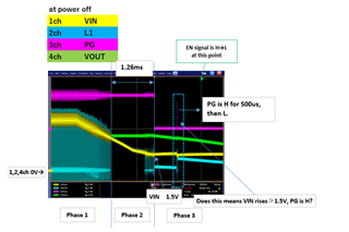
I checked the PG waveform when the power was cut off.
Could you please let me know about the operation of Phases 1 to 3

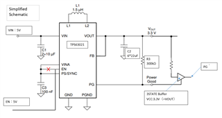
Could you please see attached the waveforms and simplified schematic below.

Phase 1

When Vin is lowered, switching stops, and there is a period of 1ms when the voltage difference between the Vin pin and the L1 pin becomes approximately 0V.

At that time, the PG terminal does not become low impedance (L signal), but maintains high impedance (H signal).

(Question 1)Does this mean that the voltage between the Vin and L1 pins is not in a current limit state?

Phase 2

Furthermore, VIN drops to around 1.5V, and after the voltage of the L1 pin switches, the PG terminal changes from High to Low impedance.

(Question 2)Does this mean that Vout drops and the TPS63021 starts switching, but VI drops and it stops operating? Is the switching mode boost? 

Phase 3

The PG pin becomes H for 500μs, and then becomes L.

(Question 3)Why does the PG pin become H?

(Question 4)Is it because VIN has risen and is now above 1.5V?

(Question 5)Are there any other conditions besides the average switch current limit that cause the PG signal to switch?

Or is the TPS63021 just observing the average switch current limit condition?

ーーー

I appreciate your great help in advance.

Best regards,

Shinichi

  • Hi  Shinichi-san,

    Thanks for reaching out, below are some comments from my side.

    Phase 1, Vin is still high or close to Vout, then device operate in buck mode first, then change to buck-boost mode. Since there is no voltage drop at Vout, would like say there is no current limit triggered here. So, yes you are correct, there s not in a current limit state voltage between the Vin and L1 pins.

    Phase2, when Vin keep goes down while Vout is stable, device change to boost mode and no switching observed in L1. but also no current limit triggered in this phase, orelse, Vo should be decreased. One unexpected behavior here is L1 start switching again when Vin is close to 1.5V. Could you Zoom in these switching cycle and also capture the current of inductor here?

    Phase 3, After unvlo_off triggered, device stop switching and Vin increase slowly, then uvlo_on and device start switching again, since no current limit triggered and vin is above uvlo_on, it is make sense PG will goes high again. Finally device shunt down by EN.

    Regards

    Tao

  • Hi Tao,

    Thank you for your reply.

    I'll share your comment with the customer.

    I ask the customer obtain unexpected waveform when Vin is close to 1.5V.

    I have additional two questions, could you please let me know. 

    (1) At the beginning of phase 3, PG went low . Is this because the UVLO was turned off?

    (2) In case of TPS63021, when UVLO_ON and current limit is not triggered, does PG goes high?   

    Does the behavior of PG going high in phase 3 indicate this? 

    I appreciate your great help and cooperation.

    Best regards,

    Shinichi

  • Hi  Shinichi-san,

    Yes, for both questions, your guess are all correct.

    Regards

    Tao

  • Hi Tao,

    I could obtain the waveform L1 start switching again when Vin is close to 1.5V.

    Could you please see attached file and advise? (TPS63021 power down(additional waveform)-1/-2/-3.pdf )TPS63021 power down (additional waveform)-1.pdf

    TPS63021 power down (additional waveform)-2.pdf

    TPS63021 power down (additional waveform)-3.pdf

    I appreciate your great help and cooperation.

    Best regards,

    Shinichi

  • Hi   shinichi,

    Thanks for your new screenshots. they are really help.

    From attached PDF, we can see operation mode is correct, only boost mode observed when vin is close to 1.5V. But there is an unexpected switching stop in this phase.  EN is always high, right? Could you help to check the status of VINA?

    Regards

    Tao

  • Hi Tao,

    Thank you for your reply.

    The device is working correctly.

    I think that the reason switching stops during boost is probably because the VINA UVLO is active.

    I have asked the customer to take capture the VINA waveform and EN condition.
    I will share when I obtain.

    I appreciate your great help and cooperation.

    Best regards,

    Shinichi

  • Hi  Shinichi,

    Ok,  Will close this thread first,  if you have further questions from customer, you can re open this thread if you want. 

    Many thanks.

    Regards

    Tao

  • Hi Tao,

    I could obtain the additional waveform.

    Although it is not below UVLO, there seems to be some places where switching has stopped.

    Could you please see attached file and advise?

    tps63021 additional waveform with PG-1 .pdf

    tps63021 additional waveform with PG-2 .pdf

    tps63021 additional waveform with PG-3 .pdf

    I appreciate your great help and cooperation.

    Best regards,

    Shinichi

  • Hi   Shinichi,

    Highlight part in PG-1 is expected, in this time, UVLO_off is triggered and device stop switching.

    I need more time to find out what happened in PG-2. Since VINA and EN are both high level(Assuming the actual UVLO for VINA is 1.5V, it is reasonable because we can see device switchinig when VINA is 1.51v)., device should not stop switching here.

    A very low possibility is  OTP triggered here, could you help to re-do this test under a low temperature.

    Regards

    Tao

  • Hi Tao,

    I talked with the customer.

    The customer agreed to close the thread with the answers given so far.

    I appreciate your great help and cooperation.

    Best regards,

    Shinichi