This thread has been locked.
If you have a related question, please click the "Ask a related question" button in the top right corner. The newly created question will be automatically linked to this question.
Tool/software:
Dear Experts,
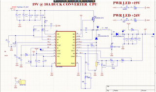
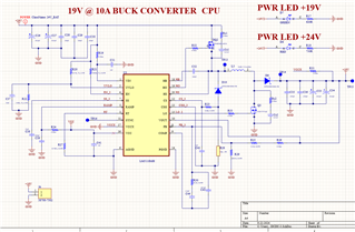
Our Requirement is having multi output DC-DC Converter,
Vin: 24V
Vout1 : 12V, 5A
Vout2 : 12V, 5A
Vout3 : 19V, 6A
i have used TI Power Design tool to generate the circuit and simulate it.
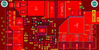
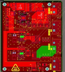
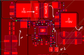
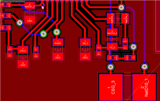
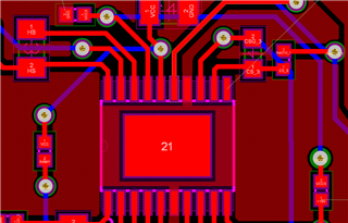
Further designed the PCB Layout which is a 4 Layout, needed a review, feedback and help


Hi,
thank you for using the E2E forum.
I just reviewed the Schematic and this this items should be fixed first before starting layout review as this will have a impact on the layout.
Best regards,
Stefan
Hi,
Stefan Thanks for your valuable feedback and suggestion,
I have done the correction as suggested,
I realized the copper pours are not proper and thermal relief is very small,
Further was wondering if the Inductor sizing is correct or not, i have used TI Workbench to generate the BOM and do the component selection.
Thanks
Tido

Hi Soumyajeet,
We do not recommend to use thermal reliefs in the layout. This will introduce parasitics to the design and the heat cannot be distributed equally over the copper plane.
The inductor size of 10uH seems to be ok for your application. What is the current rating of this inducto? Can yoshare he datashee please?
Best regards
Moritz
Hi,
Moritz points taken, once again thanks, curre rating on the inductor Irms=15.5A
www.farnell.com/.../3356787.pdf
Hi Hi Soumyajeet,
Thanks for providing the datasheet.
The inductor seems to be a good fit for this application.
Best regards
Moritz
Hi,
Moritz, Thanks for all the help, i am really grateful,
This will be my last question based on the above suggested changes, i have placed and done a layout and made the switching nodes closer and done a thick solid copper pour,
If you could just do a quick review of the layout that will be a big help, once again thanks for all the time, to provide the feedback.
1. Regarding the current sense resistor placement CS and CSG
2. Vccx Resistor Placement
3. HO, HB, HS, LO components
Marked the Input and Output side


Hi Soumyajeet,
1. The current sense resistor is part of the power stage. It is a main current path. It has to be connected accordingly:
I should have a short and strong connection to the diode as well as to GND.
2. According to your schematic, VCCX is connected to GND directly. Why is there a resistor?
3. Gate resistors should be close to the IC, not close to the FET. The bootstrap cap can also be closer to the IC.
Best regards
Moritz