This thread has been locked.

If you have a related question, please click the "Ask a related question" button in the top right corner. The newly created question will be automatically linked to this question.

BQ25887: Incorrect ICHG ADC reading and unstable converter

Part Number: BQ25887

Tool/software:

Hello, 

I'm having a couple of issues using the BQ25887 chip.

  1. The boost converter is unstable. Sometimes, seemingly randomly, the boost converter will work properly, but other times, switching will rapidly start and stop. If I lower the IINDPM register to around 1A, the converter is always stable. 
  2. Whether the converter is currently operating normally or the instability mentioned above is occurring, the ICHG ADC register does not seem to be reading properly. When I see input currents around 2.5A and the converter is switching normally, and I am expecting to see the full 1.5A default charge current into the battery, I only see a very small charge current in the ICHG register that varies from 10mA to around 100mA. With lower currents, such as when I set the IINDPM to 1A, the ICHG values do seem to become more accurate, although still slightly lower than I would expect. 

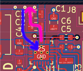
At this point I have become suspect of my PCB layout as the source of the stability issues, and am thinking that the innacurate charge current ADC value could be a symptom of the instability. I've ordered a BQ25887 EVM to see if I have the same issues on the reference hardware design. If I could get any support on confirming if the two issues are related or not, if the PCB layout is the likely cause, and what specifically about the layout needs to be improved if so, I would greatly appreciate it. 

Here are the gerber files for the PCB:

6648.battery.zip

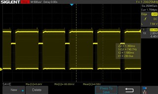
Here is a screenshot of the SW node while the instability is occurring:

Here is a register dump while the instability is occuring: 

Register Name: CELL_VOLTAGE_LIMIT, Address: 0, Value: A0
Register Name: CHARGE_CURRENT_LIMIT, Address: 1, Value: 5E
Register Name: INPUT_VOLTAGE_LIMIT, Address: 2, Value: 84
Register Name: INPUT_CURRENT_LIMIT, Address: 3, Value: 39
Register Name: PRECHARGE_AND_TERMINATION_CONTROL, Address: 4, Value: 22
Register Name: CHARGER_CONTROL_1, Address: 5, Value: 9D7D020D
Register Name: ICO_CURRENT_LIMIT, Address: A, Value: 18
Register Name: CHARGER_STATUS_1, Address: B, Value: 3B2
Register Name: NTC_STATUS, Address: D, Value: 0
Register Name: FAULT_STATUS, Address: E, Value: 0
Register Name: CHARGER_FLAG_1, Address: F, Value: 0
Register Name: FAULT_FLAG, Address: 11, Value: 0
Register Name: CHARGER_MASK_1, Address: 12, Value: 0
Register Name: FAULT_MASK, Address: 14, Value: 0
Register Name: ADC_CONTROL, Address: 15, Value: B0
Register Name: ADC_FUNCTION_DISABLE, Address: 16, Value: 0
Register Name: IBUS_ADC1, Address: 17, Value: B
Register Name: ICHG_ADC1, Address: 19, Value: 0
Register Name: VBUS_ADC1, Address: 1B, Value: 1185
Register Name: VBAT_ADC1, Address: 1D, Value: 1BF5
Register Name: VCELLTOP_ADC1, Address: 1F, Value: E60
Register Name: TS_ADC1, Address: 21, Value: 235
Register Name: TDIE_ADC1, Address: 23, Value: 5F
Register Name: PART_INFORMATION, Address: 25, Value: 29
Register Name: VCELLBOT_ADC1, Address: 26, Value: DCA
Register Name: CELL_BALANCING_CONTROL_1, Address: 28, Value: 2AF4
Register Name: CELL_BALANCING_STATUS_AND_CONTROL, Address: 2A, Value: C0
Register Name: CELL_BALANCING_FLAG, Address: 2B, Value: 0
Register Name: CELL_BALANCING_MASK, Address: 2C, Value: 0

  • Hi,

    We will check and get back to you next week.

    Thanks,

    Ning.

  • Just wanted to update - I received the EVM today, and everything is working properly with the EVM so this definitely seems like an issue with my board design. 

  • Hi,

    Have you tried a fresh new unit on your board? Does it behave the same or not?

    Thanks,

    Ning.

  • Hi Ning, I don't have any spare units right now since I ordered the boards assembled and don't have loose parts, but I do have 2 copies and both exhibit the same issues. 

  • Hi,

    Can you share a schematic? I want to make sure there is nothing wrong there.

    Regards,

    Mike Emanuel

  • Hi Michael, I have attached a pdf of the schematic to this message. Please let me know if there are any questions. battery-charger-schematic.pdf

  • Have the layout guidelines been followed?

    Can you please resend the registers? It appears as if there are more than one byte for some registers, in addition to registers missing.

    Regards,

    Mike Emanuel

  • Sorry, the registers was in a bit of a weird format. Here it is with each individual register value called out and leading zeros included. 

    Register Name: CELL_VOLTAGE_LIMIT, Address: 00, Value: A0
    Register Name: CHARGE_CURRENT_LIMIT, Address: 01, Value: 5E
    Register Name: INPUT_VOLTAGE_LIMIT, Address: 02, Value: 84
    Register Name: INPUT_CURRENT_LIMIT, Address: 03, Value: 39
    Register Name: PRECHARGE_AND_TERMINATION_CONTROL, Address: 04, Value: 22
    Register Name: CHARGER_CONTROL_1, Address: 05, Value: 9D
    Register Name: CHARGER_CONTROL_2, Address: 06, Value: 7D
    Register Name: CHARGER_CONTROL_3, Address: 07, Value: 02
    Register Name: CHARGER_CONTROL_4, Address: 08, Value: 0D
    Register Name: RESERVED, Address: 09, Value: 00
    Register Name: ICO_CURRENT_LIMIT, Address: 0A, Value: 18
    Register Name: CHARGER_STATUS_1, Address: 0B, Value: 03
    Register Name: CHARGER_STATUS_2, Address: 0C, Value: B2
    Register Name: NTC_STATUS, Address: 0D, Value: 00
    Register Name: FAULT_STATUS, Address: 0E, Value: 00
    Register Name: CHARGER_FLAG_1, Address: 0F, Value: 00
    Register Name: CHARGER_FLAG_2, Address: 10, Value: 00
    Register Name: FAULT_FLAG, Address: 11, Value: 00
    Register Name: CHARGER_MASK_1, Address: 12, Value: 00
    Register Name: CHARGER_MASK_2, Address: 13, Value: 00
    Register Name: FAULT_MASK, Address: 14, Value: 00
    Register Name: ADC_CONTROL, Address: 15, Value: B0
    Register Name: ADC_FUNCTION_DISABLE, Address: 16, Value: 00
    Register Name: IBUS_ADC1, Address: 17, Value: 00
    Register Name: IBUS_ADC0, Address: 18, Value: 0B
    Register Name: ICHG_ADC1, Address: 19, Value: 00
    Register Name: ICHG_ADC0, Address: 1A, Value: 00
    Register Name: VBUS_ADC1, Address: 1B, Value: 11
    Register Name: VBUS_ADC0, Address: 1C, Value: 85
    Register Name: VBAT_ADC1, Address: 1D, Value: 1B
    Register Name: VBAT_ADC0, Address: 1E, Value: F5
    Register Name: VCELLTOP_ADC1, Address: 1F, Value: 0E
    Register Name: VCELLTOP_ADC0, Address: 20, Value: 60
    Register Name: TS_ADC1, Address: 21, Value: 02
    Register Name: TS_ADC0, Address: 22, Value: 35
    Register Name: TDIE_ADC1, Address: 23, Value: 00
    Register Name: TDIE_ADC0, Address: 24, Value: 5F
    Register Name: PART_INFORMATION, Address: 25, Value: 29
    Register Name: VCELLBOT_ADC1, Address: 26, Value: 0D
    Register Name: VCELLBOT_ADC2, Address: 27, Value: CA
    Register Name: CELL_BALANCING_CONTROL_1, Address: 28, Value: 2A
    Register Name: CELL_BALANCING_CONTROL_2, Address: 29, Value: F4
    Register Name: CELL_BALANCING_STATUS_AND_CONTROL, Address: 2A, Value: C0
    Register Name: CELL_BALANCING_FLAG, Address: 2B, Value: 00
    Register Name: CELL_BALANCING_MASK, Address: 2C, Value: 00

    I've tried to folow the layout guidelines, the one thing I can find that I think may be an issue is my SNS loop. I have attached an image showing the current loop. Not only does it pass over a split in the ground plane right now, but the location of the vias makes it longer than it needs to be. If I reroute the trace on the backside up and around the capacitors, and move the vias to be nearer to the GND pads of the SNS capacitors I should be able to improve this loop. Do you think this could be the source of the problem?

  • Hello,

    The registers do not seem to be the problem. Can you send the gerbers so I can inspect the layout better? Seeing as this is the number one layout guideline, there is definitely a potential impact (especially seeing our EVM does not have an issue).

    Regards,

    Mike Emanuel

  • Here are the gerbers, let me know what you think! 8750.battery.zip

  • Hello,

    Please take a look at our BQ25887EVM layout. We have multiple vias down to multiple GND planes directly adjacent to each capacitor for the GND and SNS connection. I only see 5 vias under thermal pad and no via by C4 cap. C2/C3 caps have more vias further away.

    Regards,

    Mike Emanuel

  • Thanks Mike, I will take a look at the EVM example!