UCC5350: VEE2 limts for Split Outputs version

Part Number: UCC5350
Other Parts Discussed in Thread: UCC53X0S

Tool/software:

Hi,

What are the limits for VEE2 for Split Outputs version (UCC53x0S)?

In the datasheet, it says from -17.5V to 0.3V (section 6.1). However, when I look at the Typical Application (section 9.1), the split outputs version (UCC53x0S) shows a VEE2 connected signal emitter.

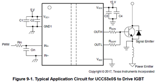
Whille versions with UVLO referenced to GND2 (UCC53x0E) have VEE2 connected to negatiive rail.

Edit / update.

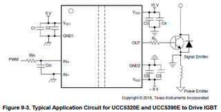
Even this datasheet shows two examples of negative bias, where Fig. 9-3 uses the split output model and VEE2 is tied to GND2, while Fig. 9-4 uses the Miller Clamp model, but the VEE2 is at negaive voltage.

Does that mean split output VEE2 must be connected to GND2 and cannot have negative voltage?

Kind regards, MB

  • Hi MB,

    Voltage is just a measure of potential between two points. The output die is isolated, so usually voltage ratings for the output are referred to VEE itself. 

    For the -E version, there is a VEE rating is referenced to GND2.  The GND2 pin is designed to connect to either a FET source or the IGBT emitter, mostly so that the UVLO can trigger if VCC2 enters a brown-out condition. VEE and GND2 can be shorted, since 0V is within the -17.5V to 0.3V rating. 

    Most important is the VCC2-VEE2 recommended max rating of 33V.

    For the split output, you can reference the VCC and VEE to the FET source=0V. In that case, you can have

    VEE=0V, and VCC=33V, 

    VEE= -3V, and VCC=30V, 

    VEE=-17.5 and VCC=15.5

    VEE= -33 and VCC=0V.

    All of these will stay within the rated VCC-VEE power supply voltage range of the split output device.

    For the E version, you would have to limit VEE-GND2 to 17.5, but that limit does not apply to devices without a GND2 pin/

    Best regards,

    Sean

  • Hi Sean,

    Thank you very much for the reply.

    In my application, I am using -3/15V; so split output would be okay...can you please check the schematic below.

    Kind regards, MB

  • Hi MB,

    That is a lot of input decoupling! One capacitor should be enough for VCCI. Have you had issues in the past?

    Also, there are many parallel Rg. Is this to reduce inductance or for to improve thermal sinking? I don't think that these will need to dissipate that much power, so you can probably get away with only one resistor.

    Usually you need a 100nF capacitor across VDD and VSS to protect the gate driver from transient overvoltage. Also, usually you need a Zener circuit to reference the floating isolated power supply to the Vsource of the driven FET:

    Best regards,

    Sean

  • Hi Sean,

    Thank you for the advice. I have added capacitors and Zener diode to Vcc2 and Vee2.

    There was no specific reason for extra decoupling capacitances between 5V and GND. I have now reduced it to a single 100 nF.

    Many Rg resistors are DNM and can be used in the future for changing/tuning Rgon and Rgoff.

    Thanks, MB

  • Looks good to me, good luck on the rest of your design.