This thread has been locked.

If you have a related question, please click the "Ask a related question" button in the top right corner. The newly created question will be automatically linked to this question.

BQ77905: LD Pin during charging

Part Number: BQ77905

Tool/software:

Hi,

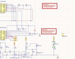
I am planning to use BQ7790518 for charging OV protection of a 8S battery pack. I have tied the LD pin of the top device to the local AVSS (top device ground). This disables the LD pin of the top device. However, for the bottom device, the LD pin is tied to a 470k resistor with a diode for protection against negative voltages at PACK-. Will my charge be detected by the LD pin in this configuration and the CHG FET will turn ON if my each CELL level voltage is in between 2.750V to 4.250V. What will happen to the LD PIN if an OV is detected? Will it clear automatically if I somehow reduce the cell voltage to less than 4.250V? Here is the schematic for your reference.

  • Also, 

    I have one more doubt regarding LD PIN.

    As stated in BQ77905 datasheet, page 24, Fig. 8-9 the top device LD PIN is connected to the local AVSS. It is mentioned "If load removal is not used for UV recovery, connect the upper device LD pin to its AVSS pin, as shown in Figure 8-9 and Figure 8-10. Otherwise, refer to Figure 9-7 for proper LD connection ". What does it meant by load removal is not used for UV recovery? What will happen If I use the LD pin for UV recovery and what will happen if I dont use LD pin for UV recovery?

  • Hi Goutam,

    Sections 8.3.2.9 and 9.1.1.4 of the datasheet explains the UV load recovery feature.

    Load detection itself is explained in Section 8.3.2.8 of the datasheet. It is just used for UV and current protection recoveries. It is not used for OV protections, so your configuration is fine.

    Regards,

    Max Verboncoeur