


Tool/software:
Hello,
Hope you guys are doing great!
I am currently designing a circuit using your (TPS7A1030PDSET) LDO.
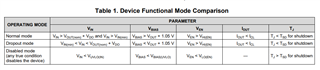
However in the datasheet it is stated that the maximum VIN is 3.3V. Furthermore, for operating in the "normal" mode, it is required that VIN >= VO(nom) + VDO. For the case of the TPS7A1030PDSET, VO(nom) is 3V, plus the VDO it raises up to approximately 3.1 V maximum.
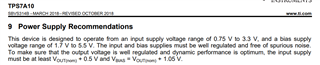
The issue comes when consulting the paragraph of power supply recommendations. There it is stated that the VIN should be VO(nom) + 0.5V. For my case, this level exceeds the maximum input voltage (3.3V).
Could you please help me clarify this? I add some images from your datasheet to illustrate my confusion.
Thanks in advance!

Regards,
Paula
