This thread has been locked.

If you have a related question, please click the "Ask a related question" button in the top right corner. The newly created question will be automatically linked to this question.

TPS25762-Q1: Troubleshooting immediate failure when USB device is connected

Part Number: TPS25762-Q1
Other Parts Discussed in Thread: PMP40934

Tool/software:

I'm having trouble bringing up a custom board and would appreciate help diagnosing the fault. When connecting USB devices to the output the regulator immediately dies with a short across the input rail. Two different boards showed identical failures with CAQ parts, and an attempt with a CQ part also failed.

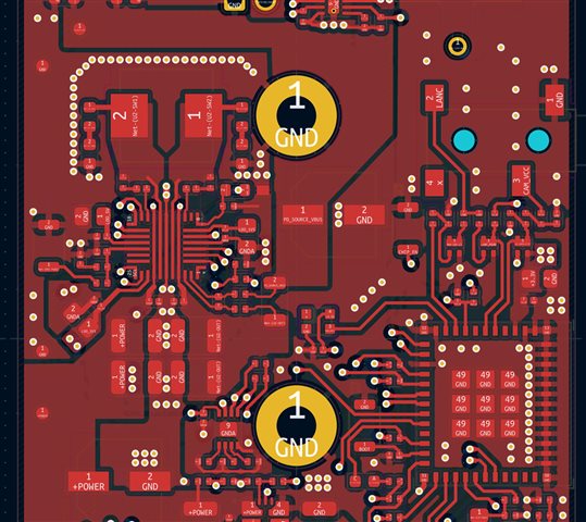
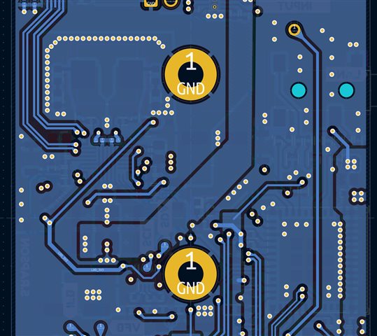
The relevant sections of the board design are attached for reference, with PDF and other relevant files in this Google Drive share.
I based the design on the datasheet reference, checked against the EVM and PMP40934 reference.

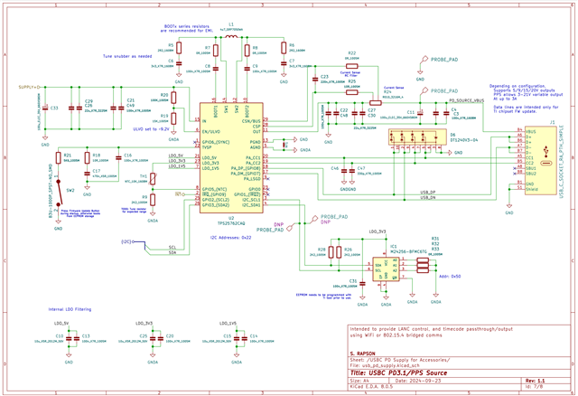
  • I can't seem to attach the configuration json file, a copy (TPS25762CQ1_V8.01_09-12-2024_11-7-30.json) is in the shared GDrive folder.
  • I manually flashed the EEPROM with a binary (base_lowregion_F311_guiCfg_5-9-58-36_full_flash.bin) generated with the GUI.
  • Validated the flashed image by dumping and comparing and it seems OK, but
    • because the binary is only 32128B, there are 640B at the end of the EEPROM which were left unwritten (0xFF).

Before connecting a USB device with the 2nd and 3rd attempts, I took a series of measurements (all with >6.5 digit SMU, truncated to relevant precision):

  • Prior to failure, the input power rail has 40-70kΩ to GND.
  • The USB VBUS net has >2MΩ to GND.
  • Using a USBC breakout board, continuity tests pass for VBUS, GND, CC1/2, DP/DM pins.
  • The input voltage is 12.05V,
  • ULVO resistors are set in design to ~9.2V - for the 12V input, EN is at 1.55V which is within expected tolerance and above datasheet threshold,
  • LDOs measured at the capacitors are at 1.55V, 3.52V and 4.65V which are within datasheet ranges,
  • TVSP pin measures open to GND (>8MΩ measured due to capacitor/strays).
  • SW1 and SW2 are ~4.2V,
  • Output voltage (USB VBUS) is 0.35V.

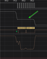
I captured the I2C traffic between the regulator and EEPROM during startup.
Transactions start ~480ms after 3V LDO is up, transactions seem fine with a quick look given there's no public docs on expected behaviour.
A Saleae Logic2 formatted save file is `tps25762-boot-eeprom-traffic.sal` in the shared folder, or I can pull specifics from the file as needed.

Notes on the failures:

  • I am using low-cost hardware as first-test devices, a 12V 'decoy' barrel plug cable with no load, and a commodity cinema lens follow-focus motor capable of 5/9/12/15V.
  • The TPS25762 fails immediately on connection. The test USB devices were undamaged.
  • There is no visible damage to the part, no noise, and no heat during the fault (guessing the PCB's input OCP kicks in, unverified).
  • After failure, the input power rail is shorted, ~0.08Ω. Removing the TPS25762 removes the short.
  • Other circuitry on the PCB seems fine once the TPS25762 removed.
  • I had a scope on the USB VBUS and input power rails for the most recent test/failure, but it didn't trigger so I have no waveform of the fault.

I have 2x TPS25762CAQ parts and 1x TPS25762CQ remaining, though without an electrical or possibly software configuration change I don't expect a different outcome.

Greatly appreciate any suggestions, a recommended bring-up procedure, or any voltage/waveforms to check which might help?

  • Hi Scott,

    I haven't download the google drive to look at the configuration yet, but I did look at everything in the thread.

    The I2C traffic shows what looks like a successful boot, so I do not see any obvious issue with your configuration.

    I am concerned about R5 and R6 being thermally capable in the system.  The seem to be 0402 case size and I don't think that will support the switching current.  Are they populated?

    Other than the size of R5 and R6, your schematic and layout look quite good, so I do not see anything on the base design that is concerning.

    Here are some questions that will help be setup a debug plan.

    Do you have an oscilloscope?

    Do you have a C to A cable?

    Is your Saleae like device analog capable?

    Regards,

    Chuck

  • Hi Chuck, thanks for getting back to me so quickly.

    I realised I didn't mention my anticipated load - it's not intended to drive more than ~30W short-duration output, typically less than 15W. The PDO configs loaded were mostly attempting to be closer to reference configurations while doing bringup/troubleshooting.

    The boards are populated as per the schematic, the details of the BOM aren't really visible but most parts should have margin on required ratings.

    The snubber resistors R5 and R6 are 0.25W rated, I agree these are a size or two smaller than reference designs.
    I can't find a datasheet value for the BOOTx currents to double-check the passives on those pins.

    • I have an oscilloscope, and a fairly well equipped electronics lab .
    • All kinds of USBC and A cables/adapters as needed.
    • Probably slightly lacking in disposable BC1.2 or PD downstream devices other than than those mentioned in the OP, but I can find/buy something with suitable behaviour.
    • The Saleae probe is analog capable, though it's only rated to 5V and ~1MHz bandwidth.
  • Scott,

    Unfortunately, you will need to attach one of your good devices to the board for debug.

    The reason I asked about the C to A cable is that it will apply Rd to CC1/CC2 to cause the PD controller to output a 5V supply without a PD negotiation.  This is the safest starting condition for the device and removes PD communication and most of the configuration controls from the FW.

    If you have a type C break out board that you can plug into the type C port that will apply 5.1K to ground on CC1 and CC2, this is equivalent.to the C to A cable.

    What I would like to see is a scope capture of VIN, SW1, SW2, and PD_SOURCE_VBUS with trigger set at 800mV rising edge so we can see the 1-5 mS of behavior after the C to A cable is plugged in.

    This will show me what is happening when the DC2DC is enabled.

    You may want to order more samples from the TI store as soon as possible so you have more devices as soon as possible.

    Regards,

    Chuck

  • No problem killing a few more parts to figure this out, I have a few more coming from Digikey.
    Not a great result with the this attempt unfortunately.

    Before attaching the USB 'device' I checked the same voltages/resistances as prior and saw the same startup behaviour. I've included some crude logic captures which include analog traces for:

    • I2C - testpoints on back of board under EEPROM
    • CC1/2 lines - probing at the 330pF cap near the USB connector.
    • LDO 1V5 and 5V - probed on the HF capacitors. I2C traces represent 3V LDO well enough.

    Seeing the same boot and initial transaction bursts as before.

    LDO sequencing:

    I2C device starts at 100kHz then increases to 800kHz. The analog SDA/SCL channels run out of bandwidth here. Sorry about the crosstalk on the CC traces.

    The test 'cable' I settled on is a USBC to USBA female adapter, externally validated to have 5k1 on one of it's CC lines (as this is typically orientation dependent).

    When I looked at the SW1/SW2 nodes prior to connecting hardware, these were DC at 4.225V. This is the BOOTx bias(?) so I'm making the assumption this is fine as we don't expect any switching prior to attach.

    I used a slightly more conservative 700mV rising edge trigger on PD_SOURCE_VBUS and the scope didn't trigger during the failure!

    The logic capture of the failure was running though. The CC1 CC2 edges match the 190ms to the datasheet trace for attach behaviour (SLVSGL9A – Fig 10.12 TypeC Attach), but ~9ms later there's that spike(likely cross-coupled?) on CC2 at the same time the LDO's all collapse.

    The rest of the capture isn't very interesting:

    • LDO 1V5 and 3V3 voltages take about 3 seconds to decay as caps discharge,
    • LDO5V holds at 500mV for exactly 820ms, then drops to ~0mV for 10ms, then sharply rises back to ~500mV.
    • LDO5V then slowly decays at ~20mV/sec for the remainder of the capture.

    I don't expect you'll need them, but the capture files for these screenshots are both in the GDrive folder.
    I can have another try, but I'll probably rethink how I'm triggering the scope as that's two failures missed - maybe external trigger set to falling edge on one of the LDO rails? Or maybe grab another scope and trigger one continuously into buffer as a fallback.

  • Scott,  

    There is something wrong on the I2C Bus on your second capture that shows the I2C.  This may be an issue with the Saleae, but the analog waveform is stuck at 1.3V according to the capture.

    I generally do not rely on Saleae except for protocol, but that is an oddity of there to look at.

    If the scope didn't trigger, then the failure may be occuring on the very first power cycle through the DC2DC.  If you try again, try triggering slightly above 4.2V on the SW1 signal.  This will be the very first action that you could detect in the power up cycle.

    I am going to put your firmware on an EVM tomorrow morning to confirm that there is no issues with the configuration, but the legacy code is not changed by configuration, so I do not expect any findings there.

    Regards,

    Chuck

  • Hi Chuck,

    Yeah I normally only use the Saleae for digital decode. The sustained mid-level there is due to the really low 1MHz bandwidth (10us) of their analog frontend just averaging the clock out.

    It's midnight here, but quickly double-checked with the scope and the I2C edges look great at 800k.

    PD_SOURCE_VBUS is the yellow CH1, SW1 is CH2 in Blue. First pulse is ~100ns duration, increase in duty slightly as they continue. ~370kHz.

  • Scott,

    I am going to review the SW1 captures with my team.  It is showing incorrect behavior on the 4th cycle.

    Regards,

    Chuck