This thread has been locked.

If you have a related question, please click the "Ask a related question" button in the top right corner. The newly created question will be automatically linked to this question.

TPS745: Layout Guideline Contradiction

Part Number: TPS745

Tool/software:

Hello team,

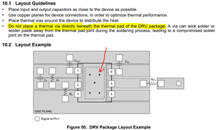
There is a contradiction for layout guideline on the datasheet.

On 10.1, it says "Do not place a thermal via directly beneath the thermal pad of the DRV package.".
However, on 10.2, the layout example shows thermal vias under the thermal pad.

Should I place the vias under thermal pad or not?

Best Regards,
Kei Kuwahara

  • Hi Kei,

    Thank you for your question.

    I found a similar thread to this exact issue:

    It's surprising to see guidance in the datasheet that recommends against thermal via's inside the thermal pad. This is one of the main methods of distributing the heat away from the device. We recommend thermal via's in the thermal pad, but you should also check with the assembly house to confirm they can meet your solder joint requirements given a PCB design. For example, you don't want the thermal vias to have a large inner diameter.

    In our local design library, we use 2 thermal vias inside the thermal pad of this LDO with 20 mil outer diameter and 8 mil hole size. More thermal vias is better if your assembly house can support it with your solder joint requirements.

    Hope this helps!

    Best,

    Hannah