Tool/software:
Hi Team
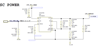
Please help to review the design below and provide your feedback.
Input Voltage: 6.5V
Output Voltage: 1.8V
Load current: 92mA

Thanks in advance,
Regards
Haritha
This thread has been locked.
If you have a related question, please click the "Ask a related question" button in the top right corner. The newly created question will be automatically linked to this question.
Tool/software:
Hi Team
Please help to review the design below and provide your feedback.
Input Voltage: 6.5V
Output Voltage: 1.8V
Load current: 92mA

Thanks in advance,
Regards
Haritha
Hello Haritha,
Thank you for your design review.
Overall, this design looks good. I just have a few comments:
Please ensure that your EN pin is 2.1V or greater to enable to device:

Additionally, I would also recheck your calculations for the feedback resistor divider network. I am calculating a R1 of about ~800 ohm for the 1.8V output, using Vfb of 1.185V.
Please let me know if you have any additional questions or concerns.
Best,
Hannah
Hi Hannah,
Thanks for the quick response,
EN pin getting signal from FPGA (Bank input is 2.5V) and for R1 Value as per datasheet i have found these equation (shown below)

In our case Vout is 1.8V and R1 is 100K, so R2=100K*((1.8/1.185)-1) = 51.89873K(~52K).
Suggest if any modification required.
Thanks & Regards
Haritha
Hi Haritha,
Thank you for clarifying the EN pin and the FB resistor network combination.
Please proceed with this design.
Best,
Hannah