This thread has been locked.

If you have a related question, please click the "Ask a related question" button in the top right corner. The newly created question will be automatically linked to this question.

TPS1HTC100-Q1: questions about stencil thickness and solder stencil opening

Part Number: TPS1HTC100-Q1

Tool/software:

Hello,

My customer has some questions about stencil thickness and solder stencil opening as follows.

Q1:
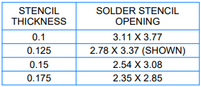
The datasheet specifies four stencil thickness according to solder stencil opening.
Which one does TI recommend?

Q2:
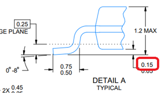
The data sheet specifies a maximum standoff (the distance from the back of the device to the PCB contact surface of the leads) of 150 μ m. In this case, is the Stencil Thickness = 100 μ m not applicable?

Q3:
Under what consideration against voids does TI specify this kind of SOLDER STENCIL OPENINGs?

Q4:
Are these open-ended openings due to concerns about the spread of wet electrodes?

Best regards,

K.Hirano

  • Hello Hirano, 

    We are working on getting these questions answered for you.

    Best Regards, 

    Alan

  • The stencil thickness is based on the PCB application that the customer has. TI provides the matching stencil opening with the customer desired thickness. In this case, it would be best to refer to the 0.15 thickness to get the most information for the customer application. This is to match what is brought up in question 2 which has expresses the limit for the device. Can you provide more information for questions 3 and 4?

    Best Regards, 

    Alan