This thread has been locked.

If you have a related question, please click the "Ask a related question" button in the top right corner. The newly created question will be automatically linked to this question.

LM5050-1: LM5050-1 unexpected behavior

Part Number: LM5050-1

Tool/software:

Hello TI team,

I would like to share with you an issue we are finding by using LM5050-1 device in our design:

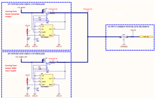
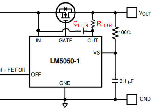
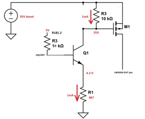
As you can see, we are implementing a OR-Ing with MOSFETs controlled by LM5050-1. Take into account that:

  • +35V_BOOST is the input of the upper OR-Ing and it comes from a boost DC/DC converter output.
  • +28_SUPPLY_FILT is the supply input of the system.
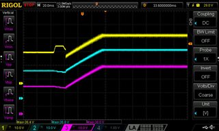
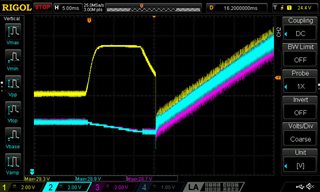
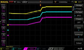
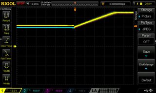
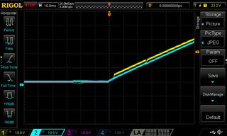
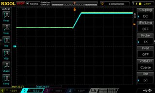
  • If 35V boost output is enabled, the common OR-Ing output should be 35V.
  • If 35V boost output is disabled, the common OR-Ing output should be 28V

We are checking the design behavior and it is not as expected:

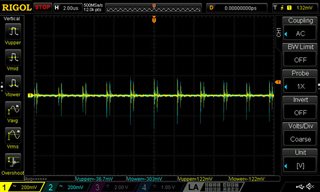
  • When 35V boost is enabled, the common output measured is 34.5V. LM-5050 gate pin voltage is measured also at 35V. That means that LM5050 controller is detecting a reverse current condition and gate pin is short circuited to IN pin (35V). Thus, the mosfet is OFF and the current flows through body diode. How could we avoid this behavior? 

Thanks in advance for your support.

  • Hi Manuel,

    Please share the waveforms.

    Measure IN(35V), GATE(U32), OUT

    Also, was the system loaded when you saw this phenomenon?

    Regards,

    Shiven Dhir

  • Hello Shiven,

    thanks for your answer. Let me take the measurments and I will come back to you.

  • Hi Shiven,

    first of all, we have observed that placing the oscilloscope probe on GATE (U32) affects to the voltage measurement:

    - with no voltage probe, we measure 40V on GATE (U32) when 35V boost is disabled ( Q19 mosfet is ON and it should not be active as we have 35V boost disabled)

    - when we place oscilloscope voltage probe, the measured voltage is 27.4V (28V - V_body_diode_boost). This is correct, and Q19 is off when 35V boost is disabled.

    Thus, just to placing voltage probe we change the LM5050 behavior.

    In addition, when we enable 35V boost, we have the following waveforms:

    CH1 (YELLOW): GATE (U32) voltage; CH2 (BLUE): IN (35V) ; CH3 (PINK): OUT

    Hereafter you can see a zoom of the same waveforms: 

    It seems that OUT signal is a little bit higher than IN signal and, thus, gate voltage is quickly discharged just when 35V boost is enabled. In this way, Q19 is off and the output is 34.5V instead of 35V (Q19 body diode voltage drop).

    Do you have any idea about this LM5050 behavior? Maybe we can add some gate capacitor to delay the gate charge as it seems like output voltage is a little bit higher than IN voltage just at 35V boost activation.

    Thanks in advance for your support.

  • HI Manuel,

    Looks like the power line is very noisy. You consider adding place holders for RFLTR and CFLTR as shown below. The RC will filter out the transients seen by the LM5050-1 reverse current threshold fast comparator but will also increase the reverse current blocking time. 

    Also, I would recommend you go through this FAQ which mentions about the leakage path in ORing.

    (+) [FAQ] LM5050-1: LM5050-1 Leakage Current - Power management forum - Power management - TI E2E support forums

    Regards,

    Shiven Dhir

  • Hi Shiven,

    Thanks a lot for your recommendation. Could you please advice us about place holder values (RFLTR, CFLTR)?

  • Hi Manuel,

    You can start with R = 100ohms and C = 10nF and increase if C if needed.

    Also, I would also suggest adding input and output capacitors to smoothen the power line.

    Regards,

    Shiven Dhir

  • Hi Shiven,

    we have implemented all your recommendations in pcb design (R, C filter from OUT to IN, added input and output capacitors and we have connected VS to IN instead of OUT). With these changes IN, OUT and GATE curves when 35V boost is enabled are as follows:

    As you can see, during the 35V boost starting up, GATE pin tries to charge mosfet gate but is quickly disabled repeatedly and finally is shorted to IN and mosfet is off, thus, 35V boost passes through the body diode again and we have 34.5V at the common output.

    In conclusion, we are not able to activate Q19 mosfet when 35V boost is enabled.

    Do you have any further idea in order to LM5050 gate output charges correctly Q19 gate and we have 35V at the common output?

  • Hi Manuel,

    Can you try to startup in standalone U32? (No Oring) Please add some load as well. 100mA should be fine.

    Regards,

    Shiven Dhir

  • Hi Shiven,

    I have tested U32 in standalone with a 150mA load and I would like to share with you the following captures:

    1. When we enable 35V boost we have:

    As we can see, just at the moment 35V boost is enabled, gate voltage (yellow curve) is quickly discharged and Vgate = Vin (Vin in blue colour is the output of 35V boost) and, thus, mosfet is cut off and common output is 34.5V after mosfet body diode drop.

    2. 35V boost disabled and we have supplied directly U32 IN from external power supply. In this case we have:

    As we can see, now the LM5050 gate output is charged around 2V higher than Vin (power supply output) and mosfet is switched on correctly.

    In conclusion, when we have 35V boost supplying LM5050 input, gate pin is discharged and mosfet is off. However, when we suppy LM5050 input directly from a external power supply, the behavior is correct and gate pin is charged and mosfet is ON.

    It seems like LM5050 is not able to charge the mosfet gate when its input comes from 35V boost.

    What do you think about this? Any solution based on your experience with LM5050?

  • Hi Manuel,

    Gate may not be rising because reverse current might be detected. Boost converters are usually noisy. Can you zoom into steady state to see behavior if voltage out of boost.

    Regards,

    Shiven Dhir

  • Hi Shiven,

    hereafter you can see boost output steady state: 35V boost output (yellow); LM5050 gate output (blue)

    If we zoom the curves we can see the noise in steady state:

    This differential noise is at the boost switching frequency (around 425KHz).  Remember we have added 100nF decoupling capacitor at LM5050 input/output.

    Do you think this noise is the root cause for LM5050 gate being not rising? 

  • Hi Manuel,

    Yes, this noise may not let the gate rise. You can try increasing CFLTR further and test again.

    Regards,

    Shiven Dhir

  • Hi Shiven,

    we have increased the value for CFLTR to 100nF and this is not solve the issue. The only thing that works is disconnecting the OUT feedback to the LM5050. In this way we get 35V at the output when boost is active. To do so we have added a circuit like this:

    This would be the solution we have found for me moment.

  • Hi Manuel,

    This circuit is just disconnecting OUT which means RCB is disabled. Can you try increasing CFLTR futher?

    Regards,

    Shiven Dhir