


Other Parts Discussed in Thread: TPS63900
Tool/software:
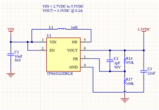
I want to design the Boost circuit using TPS61023 with input voltage range as 3.3VDC to 5VDC and output voltage fixed to be 3.3V at 200mA. Refer below schematic for your reference.
Main purpose for this design is that the Input power source should be compatible to 3.3VDC or 5VDC regulated power source and output voltage to be fixed.
At output voltage 3.3VDC, 200 mA , I have to connect two device BGM220PC22WGA2 (Bluetooth Module) and (IS25LP064A) thus total consumption will not be more than 100mA.
Inductor used is 1UH/800mA 100 mOhm.
Request you to verify the design and suggest, the best layout options.
