This thread has been locked.

If you have a related question, please click the "Ask a related question" button in the top right corner. The newly created question will be automatically linked to this question.

UCC21732: FB inverter

Part Number: UCC21732
Other Parts Discussed in Thread: UCC21551

Tool/software:

Hello Experts,

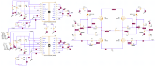
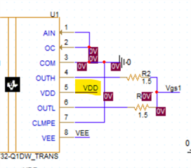
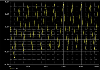
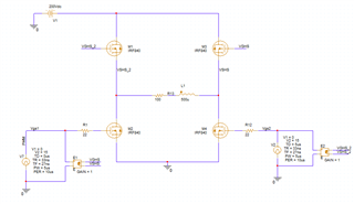
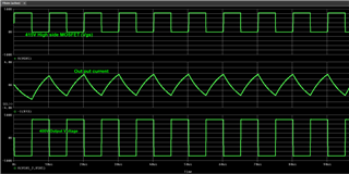
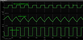
I’m working with a full bridge circuit utilizing the UCC21732 gate driver and SCT2080KE SiC MOSFETs with PSpice for TI. I applied a 400V DC input but did not achieve the expected output voltage. I was advised to use a bootstrap circuit, but I am still not seeing the desired results, possibly due to an incorrect implementation. Could you please assist me in troubleshooting and improving this full bridge inverter circuit? 


Best
Biruk


  • Hi Biruk,

    Can you share your PSPICE file?

    You are still not using a bootstrap circuit as far as I can see; your high-side gate driver still uses the same VDD and VEE as the low-side:

    Can you use a voltage controlled voltage source with a gain of 1 to create a VDD2 and VEE2 rail from your low-side VDD and VEE rails? I think that will solve the high-side power supply issue in this simulation.

    Also, you will have a lot of trouble running simulations with a Dbreak true diode model. You should use a voltage controlled switch to emulate a diode to eliminate the complexity and aid in convergence.

    Best regards,

    Sean

  • Hi Sean,


    Thank you for your quick reply. As per your request, I have shared the PSpice file herewith. How to use a use a voltage-controlled switch to emulate a diode? 


    Project8.zip


  • Hi Biruk,

    It seems you have a high expectation on what is possible to simulate in PSPICE for TI. It is really a tool for analysis of analog feedback, like op-amp circuits. There are other tools that are better suited for large switching circuits like these, such as Simplis and Simetrix.

    In order to get this simulation to work, I removed as much complexity as possible. I can drive the switches directly with the input voltage sources. Maybe this will allow you to set up a control waveform get some inductor current data. Using the gate driver models to drive the FETs like you had planned is going to be a challenge. 

    At best, you can usually simulate one gate driver model with one FET model, but even simulating one half bridge is often not possible due to convergence issues.

    Best regards,

    Sean

    Project8-2024-09-26T19-25.zip


  • Hi Sean,


    Thank you for your quick reply. Now, I got a clear understanding. 

     Does TI drivers supported by Simplis and Simetrix cause UCC21732 is an encrypted model? I want to use Simplis and Simetrix if the TI Models available.


    I would like to confirm my calculation of the gate-to-source voltage (Vgs) for high-side mosfet,

    VGHS = 195V,  VSHS = 200V


    From my understanding, the gate-to-source voltage for the MOSFET should be calculated as:

    Vgs = VGHS−VSHS = 195V−200V = −5V


    Is this correct, and is this the appropriate way to determine the gate-to-source voltage for a high-side MOSFET?

    Cause, the MOSFET with a gate voltage range specification of up to 20V.


    ~Biruk

  • https://e2e.ti.com/cfs-file/__key/communityserver-discussions-components-files/196/UCC21551_5F00_Q1.psimsch

    I made a PSIM model for the UCC21551 using a free trial license. But PSPICE for TI is the tool in which TI is invested. 

    You can still use gate driver models in PSPICE for TI, you will just have to break the simulation into parts. First, you should analyze the large signal switching using simplified voltage sources as gate drivers as in my previously shared file. This should help you understand the high-side gate drive voltages required, and you can use it to test bootstrap circuits.

    Next, you can analyze the small signal behavior when charging a single FET gate using a gate driver model like this:

    4743.UCC21750.zip

    This can help you compare the drive strength of various gate drivers, and the effect on dV/dt and switching losses.

    Best regards,

    Sean

  • Hi Sean,

    It seems the FB circuit is worked in PSPICE for TI, uploaded herewith. 

    I have a doubt with the gate-to-source voltage (Vgs) of my high-side MOSFET.

    • The Vgs of the low-side MOSFET is 15V, which makes sense.
    • However, for the high-side MOSFET, the gate voltage (VGHS) is 195V and the source voltage (VSHS) is 200V.

    I’m using a voltage-controlled voltage source for the high-side driver, and the MOSFET I’m working with has a gate voltage range specification of up to 20V. Is the high Vgs I'm seeing (415V) due to the floating voltage of the high-side MOSFET? How do I make sure the gate voltage is within the 20V range for safe operation? I am afraid this 415V destroy the MOSFET.


  • Hi Biruk,

    Sean is currently out and will get back to you by end of day tomorrow Dallas time.

    Best,

    Pratik

  • Hi Biruk,

    For the high side to turn on, it needs (Vgate - Vsource) =15. In the high-side, Vsource=400V when the switch is closed. You therefor need Vgate= 415V to keep the switch ON. Vgs is still 15V, so it will not destroy the Mosfet. Vgs is a floating voltage, since Vs is not 0V.

    Best regards,

    Sean