This thread has been locked.

If you have a related question, please click the "Ask a related question" button in the top right corner. The newly created question will be automatically linked to this question.

BQ25798: ESD protection for TS line

Part Number: BQ25798
Other Parts Discussed in Thread: , TPS25947EVM, TPS25947

Tool/software:

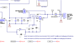
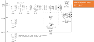
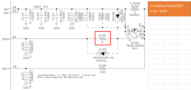
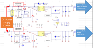
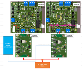
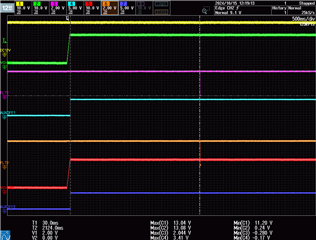
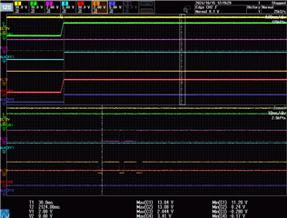
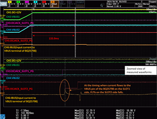
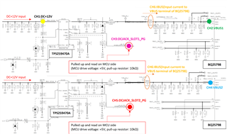
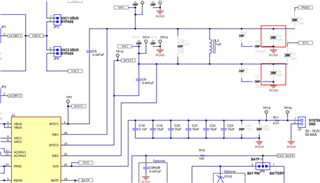
I would like to implement an RC filter circuit on the TS line of the bq25798 for ESD protection purposes. (R=100Ω, C=0.1μF)
I am considering the configuration shown in the attached circuit diagram, but if you have any concerns about this configuration, please let me know.
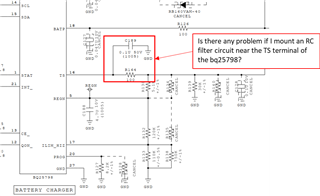


Regards,
Kagawa

  • Hi Kagawa,

    The only issue I see is delayed response (tau=3*RC) by the charger for changes in battery temp.  This includes initial charge startup.

    Regards,

    Jeff

  • Hi Jeff-san,

    As background, we are working on a design with a removable battery pack. When the battery pack is removed, the TS pins are exposed and therefore susceptible to ESD.
    With the above background, we have asked if the placement of RC filters is appropriate for ESD protection of the TS pins, and we would like to get an answer to the following questions.
    ・TI E2E below states that adding a capacitor larger than 0.01uF is not recommended. Should we change the current constant of C=0.1uF to C=0.01uF based on the responses in this thread?

    https://e2e.ti.com/support/power-management-group/power-management/f/power-management-forum/1325616/bq25798-esd-protection-bat-and-ts-pins/5077719?tisearch=e2e-sitesearch&keymatch=bq25798%2520ESD%2520protection#5077719

    Regards,
    Kagawa

  • Hi Kagawa,

    The only reason for not being recommended is due to the delayed charging turn off time when battery is hot or cold.  If the battery will not be damaged due to this delay, you can use whatever RC time constant you want.

    Regards,

    Jeff 

  • Hi Jeff-san,

    The following is my understanding of the capacitance of the RC filter for ESD protection to be mounted on the TS line in the exchange so far.
    Please confirm if this understanding is correct.

    1. The use of capacitors larger than 0.01 μF is not recommended.
        This is because the RC time constant will be larger and the time required for the charge stop to work under abnormal temperature conditions will be longer.
        As a result, charging may continue outside the appropriate temperature range.

    2. TS line capacitor capacitance limit: The maximum capacitance that can be mounted on the TS line is 0.01uF.

    3. Calculation of charge turn-off time: The delay time to stop charging by the RC filter circuit in the TS line can be obtained by the following equation:
        τ = 3 * RC (τ: time constant, R: resistance value, C: capacitor capacitance)

    Regards,
    Kagawa

  • Hi Kagawa,

    That is correct. 

    Regards,

    Jeff

  • Hi Jeff-san,

    1) Is there any problem with mounting the RC filter circuit on the TS line itself?
        If the above is not a problem, what is the maximum allowable RC time constant?

    2) In what situations do the parts (D10, C42, R16, D9) that are DNPs in the BQ25798EVM need to be mounted?
        These components are nonmounted by default, but I would like to know the design intent.


    1. please tell us how to reduce the inrush current when the battery is connected.
    2. please give me your opinion whether the circuit configuration shown in the diagram below is sufficient or whether additional components are required.
    3. what is the allowable inrush current for bq25798 when connected to battery? (BAT terminal, BATP terminal)


    Regards,
    Kagawa

  • Hi Kagawa,

    Regarding 3, 10A for up to 1s as shown below:

    Regarding 1 and 2, I have had another customer increase R125>0 ohm to slow down shipFET turn on time.  I do not recall how large of a resistor he used.

    Regards,

    Jeff  

  • Hi Jeff-san,

    1. Could you please tell me what is the maximum allowable RC time constant on the TS line?

    2. I do not fully understand the circumstances under which the DNP components (D10, C42, R16, D9) of the BQ25798EVM are required.
    Please tell me the conditions under which these four components need to be implemented.
    I would also appreciate it if you could explain the design intent that these components are placed in a non-mounted state by default.

    3. You mentioned that “R125 has been set above 0Ω to slow down the turn-on time of the shipFET.” Is it correct that this refers to R125 on the schematic?


    Regards,
    Kagawa

  • Hi Kagawa,

    Regarding 1, the TS functionality is a ladder of comparators so adding RC only slows down the comparator decision.  We do not test with RC.  The delay before stop charge is a matter of preference or possibly battery manufacturer limit for how long the pack can be HOT or COLD?  The number I previously communicated is from other customers who have used that RC and not seen issues.

    Regarding 2, if R17 is used to slow down shipFET turn on time, D10 can reduce the turn off time since it shorts R17. D9 protects the shipFET gate to source voltage from overvoltage due to SDRV too fast turn on (not a problem due to small SDRV current.  C42 simply adds to the FETs gate to source capacitance slows down turn on/off time.  I do not know what R16 is for but I don't recommend it.   

    Regarding 3, yes.

    Adding gate to drain capacitor on the shipFET will further shape the turn on time.

    Regards,
    Jeff

  • Hi Jeff-san,

    We are considering a configuration in which the TPS25947EVM is placed in front of the input of the BQ25798EVM in order to control whether the power input from the host MCU to the BQ25798 is permitted or prohibited.
    Specifically, the BQ25798EVM is assembled in the configuration shown in Figure 9-2, Single Input Connected to VBUS Directly Without ACFET-RBFET, on page 31 of the datasheet, and an eFuse (TPS259470A ) is placed on the VIN1 input side of the BQ25798EVM.
    However, the FLTb pin of the TPS259470A is falling after power input, and we are having difficulty finding the cause.
    Note that the input power source is not in an overvoltage/constant voltage/overcurrent state.
    Also, disconnecting the VBUS line of the BQ25798 and the VOUT of the TPS25947EVM will stop this phenomenon.
    Any ideas as to why FLTb falls off after power input?

    <Configuration of the actual machine>
    TPS25947EVM:
    - OVLO voltage: 15.38V detection, 13.97V return
    - OVLO voltage: 15.38V detected, 13.97V released
    - ILIM resistor: 3kΩ (input current limited at 1.11A)


    <Block Diagram>


    <Current problems>
    - The _FLT pin drops momentarily after power is input.
    - Input power is below the OVLO/UVLO/ILIM threshold.
    - The problem is solved by disconnecting the VBUS line (VIN1 pin) of BQ25798EVM and the VOUT pin of TPS25947EVM.

    <Measurement waveform>


    <Expanded figure of measured waveform>


    Regards,
    Kagawa

  • Hi Kagawa,

    Are the MUX FETs still enabled on the BQ EVMs?  Do you have a current probe to measure input current?  There will be an inrush current spike that could exceed the ILIM_HIZ setting?

    Regards,

    Jeff

  • Hi Jeff-san,

    Additional current measurement results as well as the current schematic and measurement points are attached below.

    We are unable to determine the cause of the phenomenon that the FLTb pin of each TPS259470A falls to the LOW level.
    The FLTb pin falls to LOW level 130ms after the Enable signal from the host MCU is input to EN/UVLO of TPS25947EVM.
    The resistance constant of the ILIM_HIZ pin is set to IINDPM = 1.25A.
    We have checked the measured waveforms, and we do not see any overvoltage or undervoltage conditions, nor do we see a current above the current limit specified by BQ25798 and TPS259740A.
    In addition, the waveform below shows that the FLTb pin of TPS259470A in SLOT2 goes LOW at the timing when current flows to the VBUS pin of BQ25798 in SLOT1. The reverse is also occurring.
    If the VBUS line of BQ25798 and VOUT of TPS25947EVM are disconnected, this phenomenon will no longer occur.
    Is there any possible explanation as to why FLTb falls down after power input?

    Measurement waveform
    (1) When measuring the BQ25798 VBUS terminal current on the SLOT1 side


    (2) When the BQ25798 VBUS terminal current on the SLOT2 side is measured


    (3) When measuring current at the base of the DC jack (DC12V)


    <Circuit diagram and waveform measurement position>


    The circuit configuration you have reviewed in the past, which disconnects the battery from the BAT and BATP of the BQ25798 in the event of input source loss, but when the battery is connected while VBUS power is present, an inrush current is generated from the battery to the BAT/BATP terminals of the BQ25798. (max. 18.01A, 13.53μs)
    We have heard in the past that the maximum is specified as 10A for 1 second, but is there any problem with the waveform?
    We will send you a PDF report summarizing the measurement conditions, etc. Please check it.

    <Allowable inrush current>


    <inrush current waveform>


    Regards,
    Kagawa

  • Hi Kagawa,

    The currents are inrush to charge the capacitance connected to the BQ25798 VBUS, PMID, SYS and BAT pins. 

    On the input side, I suspect the TPS25947 ILIM clamp is tripping.  If possible, I recommend setting it higher for startup and then lower after startup with a second resistor +series FET?

    On the output side, there is a path through the BATFET body diode to the SYS caps and then through the high side body diodes and inductor to the PMID diodes.  The 18A spike for 13 us is not unexpected and does not violate the 10A for 1 sec spec. 

    Regards,

    Jeff

  • Hi Jeff-san,

    The RILM resistor of the TPS259470A was set to 560Ω and the ILIM of eFuse was adjusted to 5.954A. We also measured the waveform with a 0.1uF capacitor mounted between the ITIMER pin and GND.
    However, the FLT terminal is at a LOW level and no improvement can be seen.
    The reason why the FLT pin goes LOW is unknown, even though no reverse current is seen in the current waveform.
    If the VBUS line of BQ25798 and VOUT of TPS25947EVM are disconnected, this phenomenon will no longer occur.
    Please let me know if there are any additional pins to monitor other than the waveforms below.
    Also, do you have any ideas as to why the FLTb pin drops after power input? We do not think that overcurrent is the cause.

    Measurement waveforms
    (1) When measuring the BQ25798 VBUS terminal current on the SLOT1 side


    (2) When the BQ25798 VBUS terminal current on the SLOT2 side is measured


    (3) When measuring current at the base of the DC jack (DC12V)


    This question is related to the following thread
    BQ25798: Schottky barrier diodes - Power management forum - Power management - TI E2E support forums

    https://e2e.ti.com/support/power-management-group/power-management/f/power-management-forum/1392087/bq25798-schottky-barrier-diodes

    When I inquired about the placement of Schottky barrier diodes in a previous version of this question, I was told that the diodes should be placed as close as possible to the SW and ground, and if possible, without using vias.
    However, in the BQ25798EVM, the relevant D4 and D8 are connected from the backside of the board through vias, which is inconsistent with the answer we received.
    We are currently in the process of designing the artwork and are not sure which method we should adopt for the placement of the Schottky barrier diodes.
    What is the recommended Schottky barrier diode placement?

    <BQ25798EVM schematic>


    <BQ25798EVM pattern layout>


    Regards,
    Kagawa

  • Hi Kagawa,

    Based on the plots you have sent, the charger is working as expected.  I do not expect layout to change anything.

    Regarding the diodes, on the EVM, the diodes are there to help with debug in case the internal diode fails.  If trying to use the lower Vf Schottky to improve efficiency, the diodes must be placed as close to IC pins as based, ideally on same layer as IC but if not, connected with multiple vias.  Otherwise, the Schottky does not turn on fast enough to reduce the voltage drop during the switch dead times and does not improve efficiency.

    I recommend creating another post and ask the team that supports the TPS part for help.

    Regards,

    Jeff

  • Hi Jeff-san,

    Can you please illustrate the recommended placement of the Schottky barrier diodes in the BQ25798EVM on the surface view?
    If the diodes are placed on the surface (L1 side), can you please illustrate the parts that can be moved on the BQ25798EVM layout?
    Please provide a recommended layout diagram including the Schottky barrier diodes.


    Regards,
    Kagawa

  • Hi Kagawa,

    If the diodes are only to share the inrush current at start up, then placing the on bottom like the EVM as is okay.  If bottom placement is not okay, I do not recommend moving the PMID and SYS capacitors on PCB top layer to place the diodes closer to the IC.  The high side diodes can easily be placed from PMID to SW1 and SYS to SW2.  The low side diodes require that the inductor move further away from the IC and be placed under the inductor.

    Regards,

    Jeff

  • Hi Jeff-san,

    This question is related to the following post.
    https://e2e.ti.com/support/power-management-group/power-management/f/power-management-forum/1041663/bq25798-ocp-and-ovp-timing?tisearch=e2e-sitesearch&keymatch=bq25798%2525252520ovp

    The above post answers the time between OVP and OCP detection and status change, but I would like to know the same information for the following conditions:
    1. How long does it take for the BQ25798 to report each temperature status (TS Hot, TS Warm, TS Cool, TS Cold) after the thermistor on the TS line detects a temperature change?
    2. How long does it take from the time the BQ25798 detects the insertion or removal of a battery to the status register (VBAT_PRESENT_STAT in the REG1D_Charger_Status_2 Register)?
    3. What is the time from when a valid input power supply is applied to the VBUS pin of the BQ25798 until the PowerGood status (PG_STAT in the REG1B_Charger_Status_0 Register) of the input power supply is reported?

    Regards,
    Kagawa

  • Hi Kagawa,

    Regarding 1, as shown in the block diagram, the TS function is a ladder of comparators that monitor the voltage on the TS line.  There is a 30ms deglitch to prevent chatter.

    Regarding 2, VBAT_PRESENT could take as long as charge termination detection deglitch = 250ms.

    Regarding 3, for VAC2 with MUX FET installed or VAC1 with auto D+/D- detected disabled, there is a 30ms deglitch for ACDRVx, 150ms for REGN to turn on and another 30ms for poor source detection.  For VAC1 with D+/D- with turned on, the same as above plus at least 500ms plus another 30ms for D+/D- to complete. 

    Regards,

    Jeff

  • Hi Jeff-san,

    What is the time from the expiration state of each of the following safety timers until the corresponding status bit reports 1 (Safety timer Expired)?
    1. Trickle Charge Timer (TRICHG_TMR_STAT bit in REG1E_Charger_Status_3 Register)
    2. Pre-Charge Timer (PRECHG_TMR_STAT bit in REG1E_Charger_Status_3 Register)
    3. Fast Charge Timer (CHG_TMR_STAT bit in REG1E_Charger_Status_3 Register)

    Regards,
    Kagawa

  • Hi Kagawa,

    I do not have that information but it is likely in the 100ns range.  

    Regards,

    Jeff