This thread has been locked.

If you have a related question, please click the "Ask a related question" button in the top right corner. The newly created question will be automatically linked to this question.

TPS923653: Design Check

Part Number: TPS923653

Tool/software:

Team,

Eaton is testing their LCD backlight driver using our TPS923653DRRR, see schematic below. The LCD needs 25.6V @ 40mA. The input voltage is 5V. The first issue they observed was that during open load (no LCD connected) the output of the boost converter is 63V when ADIM/HD and EN/PWM pins were pulled high. If pulled low, the device is off, so they see around 5V at the output as expected. When they connected the LCD, they  pulled ADIM/HD and EN/PWM high again and saw a little smoke out of L17 (the power inductor), so they disconnected the power supply.

They are investigating why the inductor heated up that way and at the same time wanted to ask the TPS92xxx team about it.  It looks like there's something wrong with the OVP. From previous conversations Eaton agreed to design Vout_max * R_OVP2 / (R_OVP1 + R_OVP2) < 1.1V.  In their case Vout_Max = 25.6V since they are using the boost configuration. Rovp1 and Rovp2 were designed to provide the OVP pin with 0.5V at 25.6V.

Could it be that our device is operating with high output current mode exceeding the VCC_TH?  Any feedback would be appreciated in order to help understand the root cause. 


Thanks,

Tom

  • Hi Tom,

    Our expert is OoO and he will reply to you once he is back to office, thanks for your patience.

    BR, Jared

  • Hi Tom,

    The main error in the schematic is the OVP resistor setting. Please refer to this E2E FAQ - [FAQ] How to design the OVP resistor divider for TPS923655 / TPS923654 / TPS923653 / TPS923652? - Power management forum - Power management - TI E2E support forums. This should also be the reason why customer see 63V output voltage when there is no load.

    For V_CC_TH in Figure 8-5, actually you do not need to care about this parameter if you only need to drive LED in constant-current mode. If you are interested in this parameter and want to know more, you can read this E2E thread - TPS923655: Regarding the spec of OVP - Power management forum - Power management - TI E2E support forums

    If pulled low, the device is off, so they see around 5V at the output as expected. When they connected the LCD, they  pulled ADIM/HD and EN/PWM high again and saw a little smoke out of L17 (the power inductor), so they disconnected the power supply.

    Regarding the smoke out of L17, please check if the IC get damaged during this condition or not.

    Best Regards,

    Steven

  • Hi Tom,

    The main error in the schematic is the OVP resistor setting. Please refer to this E2E FAQ - [FAQ] How to design the OVP resistor divider for TPS923655 / TPS923654 / TPS923653 / TPS923652? - Power management forum - Power management - TI E2E support forums. This should also be the reason why customer see 63V output voltage when there is no load.

    For V_CC_TH in Figure 8-5, actually you do not need to care about this parameter if you only need to drive LED in constant-current mode. If you are interested in this parameter and want to know more, you can read this E2E thread - TPS923655: Regarding the spec of OVP - Power management forum - Power management - TI E2E support forums

    If pulled low, the device is off, so they see around 5V at the output as expected. When they connected the LCD, they  pulled ADIM/HD and EN/PWM high again and saw a little smoke out of L17 (the power inductor), so they disconnected the power supply.

    Regarding the smoke out of L17, please check if the IC get damaged during this condition or not.

    Hi Steven,

    Thanks.  Customer saw some initial improvement, but circuit still does not work.  Here is the latest....

    "We have not been successful in getting this driver to work. I'll do some more testing early next week to see whether we should continue pursuing this device or what design change we need to make. Adjusting the ROVP certainly helped reducing the open load voltage (although I would expect the device to shut down instead of keeping the open load voltage). Also, the datasheet says that leaving the RFSET pin open defaults the switching frequency to 100 kHz, which in our case did not work. We had to connect a resistor. Once we connect the load, the driver stays in fault mode, pulling the FAULT pin low. The inductor also gets very hot. We have 52 boards, and I've already used three boards for investigation. Next week I'll need to get to a conclusion as this is impacting our schedule. I'll keep you posted."

    Any ideas?

    Tom

  • Hi Tom,

    Our expert is OoO and he will reply to you once he is back to office, thanks for your patience.

    BR, Jared

  • Hi Tom,

    Sorry for the late response.

    Adjusting the ROVP certainly helped reducing the open load voltage (although I would expect the device to shut down instead of keeping the open load voltage).

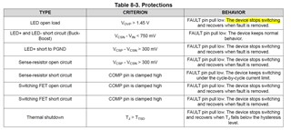
    The device will not shut down itself when open load fault happens. Please refer to Section 8.3.7 Fault Protection from the datasheet.

    Also, the datasheet says that leaving the RFSET pin open defaults the switching frequency to 100 kHz, which in our case did not work.

    This is a mistake in the datasheet. You cannot leave the FSET pin open. We will correct this mistake in next datasheet revision.

    Once we connect the load, the driver stays in fault mode, pulling the FAULT pin low. The inductor also gets very hot.

    Please show me how you change the OVP resistor and any other changes you made to the schematic. Please also show me the test setup. We can talk through e-mail if needed.

    Best Regards,

    Steven

  • Hello,

    Here is the reply from the customer:

    Section 8.3.7 says that the device stops switching when LED open load. Can you elaborate on the device not shutting down? Maybe we're mixing terms.


    Thanks for clarifying about FSET. We will continue testing with around 400 kHz, with RFSET at 59kOhms.


    About OVP, as far as I understand, we want to stay below 1.1V to keep in CC mode. I'm dismissing the VCC_TH threshold as you indicated. We changed ROVP2 from 20k to 39k and got 33V open voltage. With 20K we had 63V which was too high. Our board cannot allow more than 50V for safety. With 39K, and LCD max voltage of 27.2V, we get 1.02V at ROVP2. ROVP1 is kept at 1Meg.


    We also tested 100kHz, 200kHz and 400 kHz switching frequencies. Now I know we can't leave FSET open for 100 kHz so we will stay at 400 kHz with RFSET = 59K.


    I believe our issue is around the inductor, Csense, Rsense, and compensation network. Our calculated inductor was ~100 uH, and I've been testing with different inductors from 33uH and 330uH. 33uH (less DCR avoided overheating) seemed to behave in one board, but not in another board. The datasheet is not clear about calculating the compensation network so we are using the recommended values, but we might need to tweak them. The Vsense exceeds 0.3V in some tests. I suspect our wirewound Rsense is problematic, so I'll test with another resistor non-wirewound. Adding more capacitance to Csense helped in one board, but not in another. In one board, the IC went bad (VCSP - VCSN shorted). In another board, the compensation capacitor went short. As you can see, I'm getting conflicting information. I will do more testing today on clean boards and let you know. We can have a call to go through the details of our testing. Clearly, we have some serious issues. I believe we just need to find the right values for our configuration where the calculated ones don't necessarily work.

    ***Edit 10/9 - New info received following last post.***

    Customer did the following

    1. Changed ROVP2 to 39k to reduce open load voltage.
    2. Increased Csense to 20.2uF.
    3. Changed inductor to 56uH
    4. Changed resistor type to avoid the inductive properties of wirewound.
    5. Added another 1nF in parallel with Ccomp.


    With these changes, Vsense has a voltage drop of 0.2V and the output voltage for the LCD is within range (24V). However, if we look at the switching node with the scope, it's switching at around 3 MHz when RFSET is 59k and we expect something around 400 kHz. So something seems to be wrong still.

    Thanks,

    Tom

  • Hi Tom,

    Section 8.3.7 says that the device stops switching when LED open load. Can you elaborate on the device not shutting down? Maybe we're mixing terms.

    When I said "shut down" in my last post, I meant to say the device enter into "shutdown mode" where the device is disabled (in the same manner as you disable the device by holding the EN/PWM pin low for a period that is longer than t_PWM_IN_OFF). When LED open fault happens, the device stops switching but is not disabled.

    Please try to do below modification in a board with the default setting as shown in the above schematic - 

    • Change R243 to 39kohm
    • Change C183 to 0.22uF
    • Change R241 to a resistor of a suitable type for current sensing
    • Enlarge C185 to larger value like 10nF
    • Reduce R245 to a smaller value like 200ohm

    Please have a try and see if this helps.

    By the way, have you ever tried these settings on the EVM? If so, then does it work?

    Best Regards,

    Steven