Other Parts Discussed in Thread: BQ40Z50, BQ27542-G1
Tool/software:
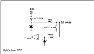
I ask this question recognizing that the BTP_INT pin of the BQ40Z50-R2 is push-pull.
1) Please provide information on the buffer configuration of BTP_INT.
(power supply, resistor values, etc. for internal pull-ups of BTP_INT)
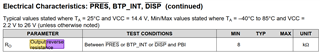
2) Please inform us of the maximum output voltage of BTP_INT.
3) Please explain the following points regarding the external pull-up of BTP_INT.
- Power source to be used
- Restrictions on pull-up resistor values
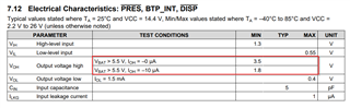
(See the yellow portion of the figure below on p. 25 of the bq40z50 data sheet.)
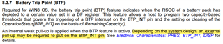
4) Please explain the meaning of Ro (Output reverse resistance) and specifically which part of the resistance is indicated.
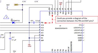
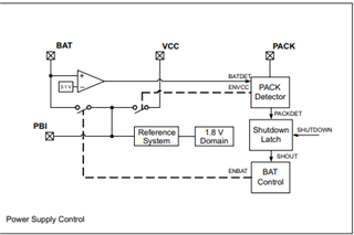
5) Am I correct in understanding that the PBI pin normally outputs the same voltage as the BAT power supply?
As background, we have just applied BAT power to a bq40z50 evaluation board and have confirmed that the PBI has the same voltage as the BAT power supply.
Please confirm this understanding.
Regards,
Kagawa