This thread has been locked.

If you have a related question, please click the "Ask a related question" button in the top right corner. The newly created question will be automatically linked to this question.

LM27762: VFB- out of spec

Part Number: LM27762

Tool/software:

Hi,

I am trying to evaluate LM27762 design to generate +/- 5V from 5.2V input voltage. 

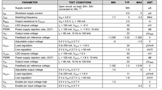
I have observed that voltage at VFB- pin is out of spec.

Please find following design values 

Vin = 5.2

For +ive voltage 

VFB+ = 1.20

R1 = 220K , R2 = 68K

Vout+ = 5.07

for -ive voltage

VFB- = -1.15 ( out of spec as per datasheet )

R3 = 270K , R4 = 82K

Vout = -4.99


I am not sure if voltage divider can affect VFB- voltage ?

Can you please share what can affect the -ive voltage output. 

Regards,

Anurag

  • Hi Anurag,

    Vout is specified from ±1V5 up to ±5V, are you trying to get a higher output voltage?

    Regards,

    Frank

  • for my application i need to generate +/-5V. 

  • Hi Anurag,

    There will be some voltage drop across the charge pump output impedance as well as the LDO dropout voltage. The LM27762 charge pump used for the negative rail has a certain output impedance. Please see figure 4 in the datasheet on how the output impedance varies over load current. You can measure the voltage at the output of the charge pump by measuring the voltage across the cap connected to the CP pin.  Could you let me know how much load current you have on the -ve rail? Another voltage drop to consider is the drop out voltage of the LDO used for the negative rail. Please see figure 3 in the datasheet for these curves. 

    Best regards,

    Varun

  • Hi Varun,

    Please find following values 

    Vin (V) I_load (mA) Vout (V) CPOUT Voltage (V)
    5.2 5 -4.98 -4.98
    5.2 10 -4.98 -4.98
    5.2 20 -4.96 -4.96
    5.2 25 -4.95 -4.95
    5.2 50 -4.9 -4.9

    Regards,

    Anurag

  • Hi Anurag,

    Looking at the curve in figure 4, around 200mV drop across the charge pump is expected at 50mA load current. You measure around 300mV drop. Is the 5.2V input measured close to the IC VIN and GND pins? I am not sure if the extra 100mV is coming from PCB drops. 

    Is it possible for you to change the input supply in your design to 5.5V instead of 5.2V? I think that would give enough margin for the converter to regulate correctly.

    Best regards,

    Varun