Tool/software:
Hi! I am currently working with the TPS25751 power delivery module, and i am reviewing the PATCH to APP operation and reading the document slvafv8 (Application Note
Common TPS25751 Use Cases and Setting Using EC) I have the following question:
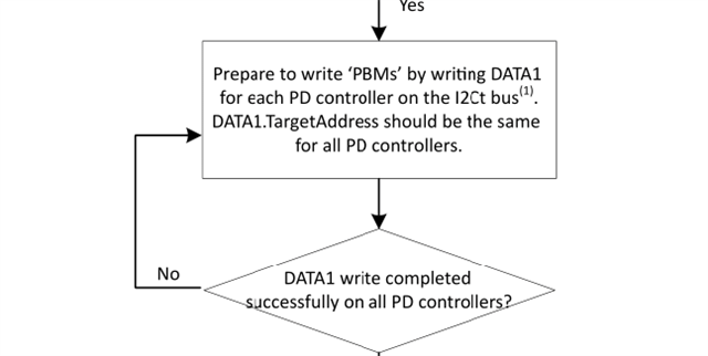
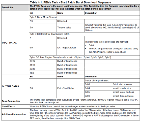
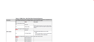
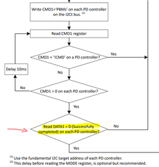
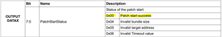
In the first pic i have attached, it says to write 'PBMs' by writing the DATA1 register and in Table 4-1 (second pic attached, it says that the register has the structure indicated in pic nº 2.
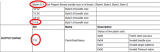
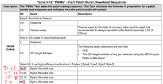
But i don't know where output data is located, because in the Input data section, it says that Bytes 0-3 are the Low Region Binary bundle size ( 4 Bytes) but the LSB of this pack of 4 bytes it says bits 15:8 are Byte1 of bundle size.
However in the output data section it says bits 7:0 are Output data so it would seem that Byte 0 is the one reserved for output data but i am not sure, since it could be that Byte 0 is input data according to the Bytes 0-3: Low Region Binary bundle size in of bytes.
If anyone could clarify it would be great!
Thanks in advance!
Juan