


Other Parts Discussed in Thread: BQ25798, USB2ANY
Tool/software:
Hello! I've been working on a Sodium-Ion battery charger based on the BQ25798. The designed is completely based off the EVM, however I removed the SHIPFET as it stopped the charger from working for some reason, as seen in this forum. The problem is that after I made and validated that the EVM design works (PCB#1), I made another PCB without any of those annoying jumpers (PCB#2) and did the connections just as I configured them on PCB#1. Long story short (more like shorted), this PCB has sent about a dozen chips to heavens. Could you please look at the original schematic (PCB#1) and the new schematic (PCB#2) and tell me if I mis-connected anything?
Before reading the schematics, here's how I determined chips were dead: 50% of them had REGN and GND shorted, 50% of them were drawing more current than usual and could not connect to the EVM GUI in cloud, OR were attempting to start (current going up to like 10-30mA), but failed to start and would go back to 0.
From the good PCB (PCB#1), I determined that a working board should draw about 6mA at 5V, decreasing to about 2mA at 20V input. Bad PCBs would usually draw 10-150mA.
All tests were supplied by an adjustable CC/CV bench power supply.
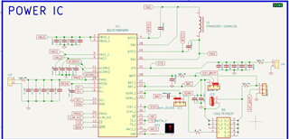
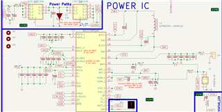
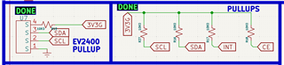
Schematic one, jumper connections are marked with red lines across pins:
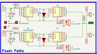
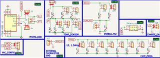
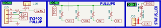
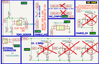
Schematic 2, jumpers removed, parts crossed in red is nor mounted on the PCB, CE is connected straight to GND with a 0O resistor:
I know I should've asked this a long time earlier... But please, if you spot any difference between the connections that I made on PCB#1 with jumpers and I made on PCB#2 wrongly, then let me know. Or any design issues that I may have.
Also, I just moved all parts to a brand new PCB, properly soldered them, and right now my current chip does indeed draw current (PCB#2), has 5V on REGN regardless of input voltage (5-20V), however it makes a very weird switching noise, its STAT pin blinks at 1Hz and it draws a varrying current (not constant) of 18-25mA... At this point I said stop, there may be something wrong I'm doing.
Also, with the EXACT same setup (PCB#2), i managed to make it work twice today! (the pcb drew 6mA at 5V and 2mA at 20V) It was perfect, 5V on REGN, good current, we could connect to it in the GUI and read ADC values/write to it with the USB2ANY, simply heavens. But then... I power cycled it and it once again started drawing 20-40mA and I could no longer connect to it with I2C. I don't think this is a problem of "not all pins are properly connected", but more like a component or trace exists where it shouldn't.
There's a lot of possible issues... Bad connections, solder bridges... However I just inspected my current PCB version and it has the best connections I've seen on the BQ chip, and yet it's singing its frequency song to my ears. What should I do? One thing I did not mention was that instead of a 2O snubber resistor I use 2 x 3.9O in parallel as I didn't have a 2O one.
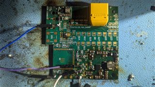
Here's how the PCBs look like.
PCB#1 (good, works perfectly, 6mA at 5V):
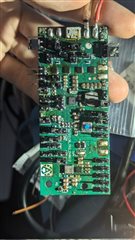
PCB#2 (switching noises, graveyard of BQs):
So far my approach to solve this issue was: "Solder it again". "Hot air it again", and again, and again, with a 60% chance of getting the exact same problem, thus no result, and 40% chance of getting another problem or damaging the chip, then replacing some parts after a couple hours of trying with brand new ones. This doesn't go anywhere
