This thread has been locked.

If you have a related question, please click the "Ask a related question" button in the top right corner. The newly created question will be automatically linked to this question.

TPS25730: TPS25730 FAULT_IN behaviour

Part Number: TPS25730

Tool/software:

Hi,

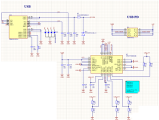
I'm trying to understand the FAULT_IN pin's behaviour.

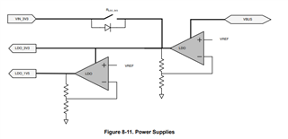
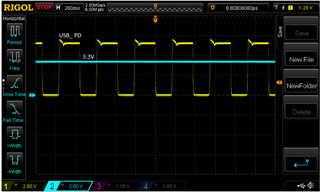
When the TPS25730 is supplied by 5V USB 2.0 source, the chip lets through the 5V even if the FAULT_IN pin is low. Is this normal behaviour? Also, once the FAULT_IN is set to HIGH and then set back to LOW, the TPS25730 does not cut-off the usb power to the internal circuit.

Thanks,

Tamas

  • Hi Tamas,

    The FAULT_IN pin is an active low pin that put's the PD controller into a Type-C Error recovery state. It should disable the CC lines and power path.

    How are you determining that "it does not cut off internal power". Are you seeing power draw at PPHV?

    One thing to note is USB 2.0 is active hot, which means there will always be 5-V on VBUS irrespective of the CC line behavior. Type C first waits for the correct biasing on the CC lines before providing voltage on VBUS. The TPS25730 should not be closing the power path if there is nothing on the CC lines.

    Thanks and Regards,

    Chris

  • Hi Chris,

    Yes, there is power draw at PPHV. Today I figured more. So we either supply USB 2.0 or Type C. USB 2.0 indeed is always 5V. And the TPS25730 lets through the 5V through PPHV when FAULT_IN = LOW. Is this normal behavior? Can it be altered through I2C?

    Another thing. In Type C, if we pull FAULT_IN = LOW, the higher negotiated voltage will stop existing from the source. However, the source starts outputting a squarewave of 5V, with a period time of 400ms. That also goes through PPHV while FAULT_IN = LOW. Is this also normal behavior?

    Thanks,

    Tamas

  • Hi Tamas,

    Is the system VBUS powered or do you have internal power to VIN3V3?

    I'll need to do some testing on my end, this seems like it may be expected due to the behavior of the PD controller in Dead battery mode.

    Thanks and Regards,

    Chris

  • Hi Chris,

    No internal 3V3. Everything powered by USB. 

    Please schematic part copied:

    Thanks,

    Tamas

  • Thanks for the information,

    How is Fault_In being biased? Is it directly tied to ground? Or to a GPIO?

    Give me a couple days to test and the lab and get back to you.

    Thanks and Regards,

    Chris

  • Hi Chris,

    It has a pd resistor, then if a button is pressed, a discrete circuit pulls up to about 2.2V and latches there.

    When we want to turn off the device, a GPIO turns-off the latch circuit and the FAULT_IN goes back to 0V.

    Thanks,

    Tamas

  • Hi Chris,

    Today following more measurements, I can confirm it is the dead-battery feature of the chip making the behavior. Having supplied 3.3V separately to VIN_3V3 can make the FAULT_IN = LOW turn off the VUSB in all cases. 

    So we are considering different solutions, to solve our quiescent current from VUSB power banks, as it would be our goal.

    1) We have a small 100mAh Li-ion battery in our application for RTC retention reasons, that could be used to always supply VIN_3V3.

    2) We just tie our internal LDO 3.3V output to VIN_3V3 and FAULT_IN. And we try to minimize our quiescent current consumption by additional trying to turn off all internal hardware circuits on our board and putting the microcontroller in deep-sleep

  • Hi Tamas,

    I did a quick test with an EVM and saw similar behavior.

    I'll describe what we think is happening to hopefully provide some clarity.


    From "dead battery" (power is coming from the Type-C connector), we are capable of exposing pulldown resistors on the CC lines to advertise the port as a USB-C Sink. Once this occurs, the USB-C source(i.e. a wall adapter) will see the pulldowns and provide 5-V on VBUS. VBus will then provide power to the PD controller, allowing it to boot, read the ADCIN resistors, and also monitor the GPIOs. The issue you are currently seeing (without VIN3V3 power) is that on dead battery boot, we default to closing the VBUS->PPHV power path, so the 5V from VBUS feeds through to PPHV.

    Then, when we power up, we notice the fault_in pin is asserted and will execute "Type-C error recovery" due to the pin being asserted. Type-C error recovery is handled by changing the CC pins on the TPS25730 to HI-Z to indicate to a type-C source that there is a disconnect. By setting the CC pins to Hi-Z, we remove the pulldown resistors mentioned above that advertise our port as a USB-C Sink. The source will notice this, and (if it is a USB-C or USB-C PD source) it will remove VBUS, which in turn causes the TPS25730 to lose power.

    At this point, it basically looks like a cable detach and the system will restart from the beginning, which is why you see the constant cycling of power.

    Unfortunately, this specific case does not have a solution, and you may need to power VIN3V3 to get the desired behavior.


    1) We have a small 100mAh Li-ion battery in our application for RTC retention reasons, that could be used to always supply VIN_3V3.

    This could work, but you would need to account for power draw.

    2) We just tie our internal LDO 3.3V output to VIN_3V3 and FAULT_IN. And we try to minimize our quiescent current consumption by additional trying to turn off all internal hardware circuits on our board and putting the microcontroller in deep-sleep

    You will still end up having the same issue as the LDO_3V3 is generated from VBUS. The moment you trigger error recovery and lose VBUS, you lose LDO3V3 and will continue to see the power cycling.

    3. ------

    This is just a thought, but you may want to move this latching behavior to a part of the powerpath downstream of the TPS25730? I don't know your intended use of this pin, but it may be simpler to rely on another part of the system that manages the power path if the FAULT_IN behavior does not meet your requirements.

    Thanks and Regards,

    Chris

  • Hi Chris,

    Thanks for the detailed answer, really helpful.

    We are investigation what to do, will post here soon.

    Regards,

    Tamas

  • Hi Chris,

    Thanks for the detailed answer, really helpful.

    What is interesting in our application, even when the USB PD source is outputting a cycling 5V, our internal LDO is establishing a stable 3.3v like this:

    So therefore I think actually tieing our internal 3.3V to the FAULT_IN and VIN_3V3 seems to work.

    We are doing further investigation, will post here soon.

    Regards,

    Tamas

  • Hi Tamas,

    Thanks for the update.

    Where are you measuring the toggling voltage? VBUS, PPHV?

    How are you powering your system for the capture above? Do you power VIN3V3 or is this still dead battery?

    If you start in dead battery, we will power cycle on losing VBUS voltage (due to fault_in).

    Thanks and Regards,

    Chris

  • Hi Chris,

    The measurement is on VBUS, and the USB PD source is outputting this toggling 5V there. At the same time we have similar signal patterns existing on the CC line.

    In this measurement, the VIN3V3 was still left unconnected , so yes it was dead battery mode.

    For me it seems, even though there is power cycle of 5V in dead battery condition, it is let through PPHV and it is enough for our system to boot up (90mA consumption).

    The 3V3 on the oscilloscope picture is the internal 3V3 of the system, it is not the VIN3V3 of your chip.

    Thanks,

    Tamas

  • Hi Tamas,

    Got it, yeah, when booting in dead battery, we will reset whenever we see VBUS drop (this happens due to Fault_in assereted) so the toggling is expected.

    Thanks and Regards,

    Chris

  • Moving forward, we would like to achieve low quiescent current in our application when we are at sleep.

    I have understood from the datasheet, when the USB PD chip is awake, it can consume ~3mA typical from 20V. In our application we want to use it from 9-15V. Do you have additional typical consumption (if possible up to 40°C) data for those USB voltages as well?

    Thanks,

    Tamas

  • Hi Tamas,

    Let me check with the team, but I do not know if we have those application curves.

    Thanks and Regards,

    Chris

  • Hi Tamas,

    Regarding the quiescent current information, that is all the data we have. 22-V is the worst case.

    Thanks and Regards,

    Chris

  • Thanks Chris!

    Unfortunately the GPIOs are loaded with resistors as well and I need to involve them aswell in the calculation. I am analysing max resistance I can put there without jeopardizing the ADC measurement due to ADC pins' input leakage current. In datasheet this current is +- 1uA for full temperature range. We have only a temperature range of 0°C to 40°C ambient. Do you have any unofficial tighter temperature range measurement for that leakage current?

    Also, is that leakage current already involving the ADC periphery's internal sampling capacitance?

    Are the I2C pins needed to be pulled up if the I2C function is not used in our application?

    Thanks,

    Tamas

  • Hi Tamas,

    I am checking with the team on the ADC related questions.

    Are the I2C pins needed to be pulled up if the I2C function is not used in our application?

    The I2C pins can be grounded when unused.

    Thanks and Regards,

    Chris

  • Hi Tamas,

    In datasheet this current is +- 1uA for full temperature range. We have only a temperature range of 0°C to 40°C ambient. Do you have any unofficial tighter temperature range measurement for that leakage current?

    We do not have any unofficial tighter measurements for that leakage current. When speaking with the team, it was reinforced to be careful getting too close to the ADC thresholds while increasing the ADCIN resistance as you noticed.

    Also, is that leakage current already involving the ADC periphery's internal sampling capacitance?

    We were not entirely sure what you were asking here, but the leakage current spec does account for normal runtime.

    Thanks and Regards,

    Chris