UCC28070: Offset methode

Part Number: UCC28070

Tool/software:

Hi team,

I have two questions.

1.As in the reference circuit, current sensing is done with a resistor.
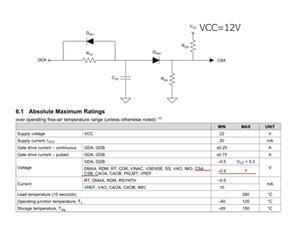
Input to the CS pin is via an op amp, but in the worst case, VCC is input to the CS pin.
Since VCC is used at 12V, will it be destroyed if it exceeds the maximum rating of the CS pin?

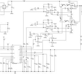
2.In the offset circuit example in the data sheet, it is pulled up to VCC, but is it okay to pull it up to a voltage higher than the CS pin's rating?

Best regards,

  • Hello Hirotsugu-san, 

    For your question 1:
    Yes, the UCC28070 can be destroyed if CSA and CSB input voltage exceeds 7V, as you show in your 2nd question. 
    I avoid this possibility, I suggest to reduce the V+ bias voltage on U3A and U4A by inserting a small-signal NPN transistor (such as 2N3904 or similar) between VCC and V+.
    Collector to VCC, base to VREF, emitter to V+ on U3A and U4A.  That will limit the CSx op-amp outputs to VREF-0.7V = ~5.3V.   

    For your question 2: 
    The pull-up resistor Roa does go to VCC, but its value is in kilo-ohms, while the normal current-sense resistor Rsa value is in low ohms.  This effectively forms a voltage divider with attenuation in the neighborhood of VCC/~1000 (or similar).  So the offset voltage applied to CSA and CSB is usually ~100mV or so. 
    Roa cannot pull up CSA all the way to VCC unless Rsa is open. 

    Regards,
    Ulrich 

  • Hi Ulrich,

    It says that VREF should be used at 2mA or less, but is it okay to connect it to base?

  • Hi Hirotsugu-san, 

    Yes, it is okay to connect the base of the BJT to VREF.

    Since the total VCC current for the two op-amps will probably be around 10mA or less and the Vce of the NPN will be >5V, the hFE of the device will be very high even at cold temperatures.  I expect typically > 50, so Ib will be < Ic/50.  Base current loading on VREF will be much much less than 2mA.  

    Regards,
    Ulrich