- Ask a related questionWhat is a related question?A related question is a question created from another question. When the related question is created, it will be automatically linked to the original question.
Tool/software:
I'm bringing up a new design which has 3 devices attached to a common I2C bus.
I am using SMBus byte read/write commands and able to talk to the CSR's and read known reset values so that is all good.
My hardware has nSLEEP pulled to 3.3v, and ENABLE is a GPIO controlled pin I have pulled high.
I've programmed MON_CH_EN (0x1E) to 0xff and VRANGE_MULT=4
When I read a monitor channel I have hooked up to a test point and external power supply, I am always reading back 92 decimal.
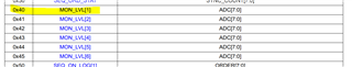
I am writing 1 to the BANK_SEL register and then readint the MON_LVL1
I am always reading back 92. I am not sure if my sequence above is correct.
Why can I not see any change in the MON_LVL register even if I change the input voltage?
What is a strategy to debug here?
Thank you!