Tool/software:
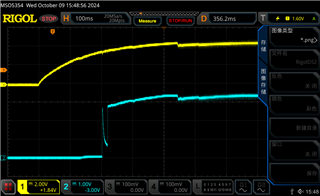
We used TPS54j061 to convert 5V into 3.3V, and we used resistor voltage splitting to convert 5V into 1.7V and provide it to the EN pin. However, in our actual use, the 5V power supply was too slow to power on, resulting in VIN equal to 3.58V when the EN pin reached the opening voltage of 1.22V. Since there is no VCC input in this design, it will still take some time for VIN to reach 4V, during which 3.3V output will drop. Regarding this phenomenon, we would like to use the following solutions:
By means of resistor voltage divider, the 5V is divided into 1.5V and supplied to the EN pin, so as to ensure that when the EN pin level rises to 1.22V, the VIN is equal to 4.0V, and the 3.3V level can be stably output. However, since Venl=1.0V, the margin of Ven is only 0.5V. Can this design guarantee the stable operation of TPS54J061?


