This thread has been locked.

If you have a related question, please click the "Ask a related question" button in the top right corner. The newly created question will be automatically linked to this question.

UCC28951-Q1: Previous Post , B Fet NOT turning OFF/ Turning ONN at proper instant.

Part Number: UCC28951-Q1

Tool/software:

Hi Mike,

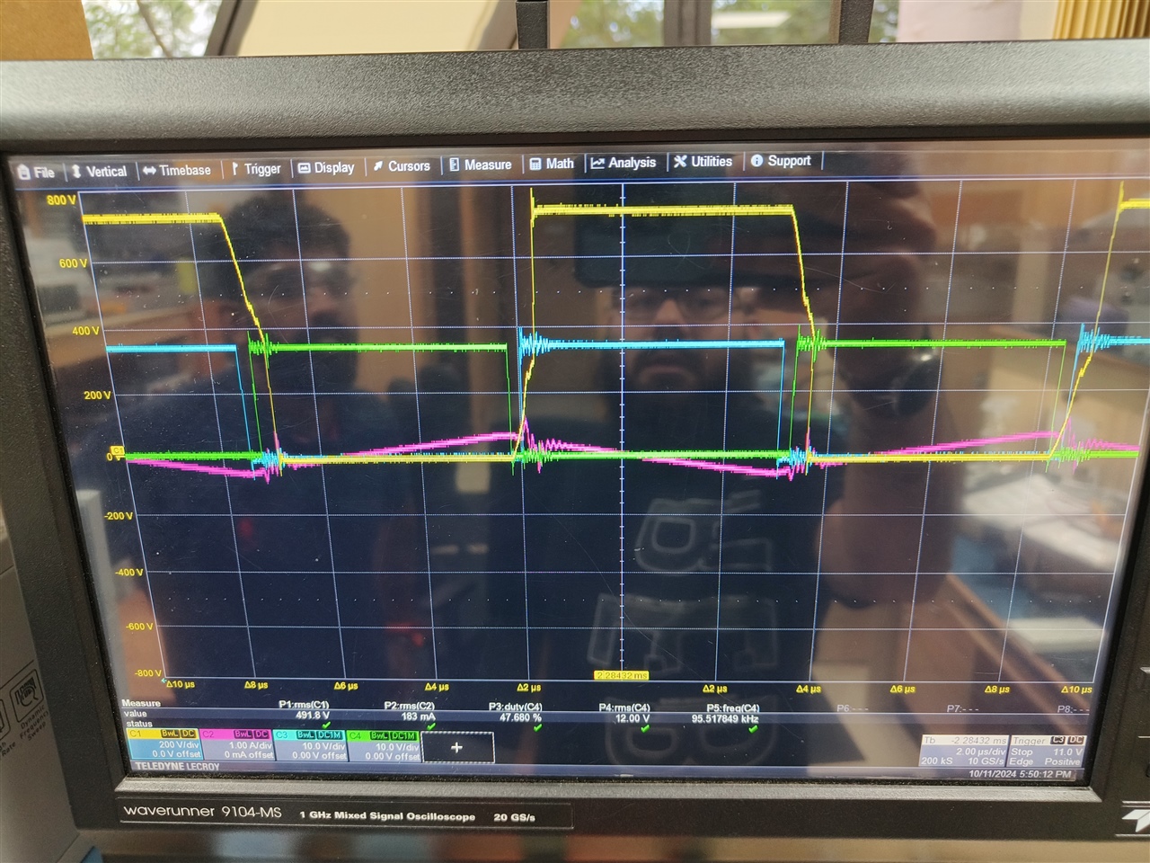
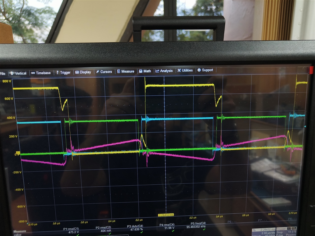
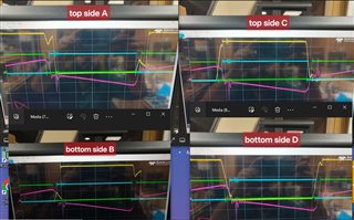
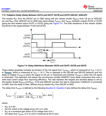
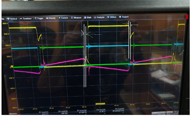
As per application note, and previous post, TABSET, TCDSET should be equal. SInce now we are using only fixed delay option. Adaptive delay is not being used as suggested.

I have set more dead-time just to understand the issue. D Fet Turns OFF / turn ONN properly, coinciding with One of the synchronous gates( Blue ). Whereas B drain to source waveform if you observe, it tries to turn OFF / Turn ONN, but something is preventing it. Should I try adaptive delay option or should i continue with fixed delay option. Is it something to do with Leakage of transformer ? Kindly suggest. 

  • Hello,

    Your inquiry has been received and will be reviewed shortly.

    Regards,

  • Hello,

    The fixed delay approach should work for your application.

    What TABSET and TCDSET delay do you require?

    Could you take scope plots and of QBd and QDd and measure 1/4th the resonant ring period?

    This should be the delay you need.

    Regards,

  • Hello,

    I adjusted delay and below are results.have captured synchronous FETs gate and B drain to source. 

    load :1A , Vin : 700

    Load : 5A, Vin : 700V

  • Hello,

    Your inquiry is under review.

    Regards,

  • Hello,

    I am having an issue posting graphics into this file.  I am not sure why this is an issue and I will report it to the e2e team.

    Your FET A through FET D turn on delays should be set for 200 ns.  It looks like your turn on delays are set for 600 ns.  Could you try adjusting the turn-on delays to see if your waveform improves.

    Regards,

  • Hello,

    1. I tried adjusting DELAB, DELCD keeping DELEF Contant, what i notice DELEF also reduces If i Change DELAB, DELCD. Why is that? Even though i did not change DELEF resistor.

    2. Below is a waveform comparison of primary FETs w.r.t. synchronous Fets Gate pulses ( Previous Reply Problem summarized )

    3. Even i have trouble pasting pictures, using chrome browser for now.

  • Hello,

    The turn on delays of E and F is based on the turn off A and B.   If you are using adaptive delays the E and F delay will move with the CS signal.

    If you are using the fixed delay approach.  ADEL and ADELEF will be either grounded or setup with a voltage divider between VREF and the ADEL ADELEF pins to ground.  If you change the turn on delay of RAB and RCD with out changing the voltage at ADEL and ADELEF it the turn on delays of E and F should not be changed.  However, if somehow you are changing the voltage at ADEL and ADELEF you will change the delays.  I would check to make sure that you are not adjust the voltage at ADEL and ADELEF to adjust the TABSET, TCDSET timing.  You should just need to adjust the RAC and RCD resistors.

    You still need to set the turn on delays of A, B, C and D to remove the original issue that you are seeing.  

    Regards,

  • Hello,

    For now I'm only using fixed delay approach. ADEL, ADELEF are grounded. I tried reducing DELAB, DELCD, to lower values, what I notice is DELEF is also reducing which I didn't understand. I reduce DELAB and waveforms slowly started to become clean, but then I noticed DELEF somehow gets reduced and It's like removing problem from one side and adding another problem. 

  • Hello,

    The turn on delay of OUT F should be based on the delay set by REF and the turn off of OUT A. 

    The turn on delay of OUT E should be based on the delay set by REF and the turn off of OUT B. 

    If ADEL and ADELEF are both grounded, I would not think that that changing RAB and RCD would have an affect when OUT E and OUT F go high.

    Did you verify this at Out A, Out B and Out E and Out F of the controller?

    The only thing that I think could think of that may be different.  Is If you decrease the turn on delay of Out A .. Out D.  This will increase the maximum duty cycle that is achievable.  The behavior of out F and E will change based on this.  However, they should still be turning on based on OUT A and OUT B going low.  Please note that Out E and Out F will be high during the free wheeling periods.  

    Regards,

  • I will share Some images of the testing later. I want to understand few things.

    1. Share me data for doing PSFB using SIC mosfets. Presently For next revision schematic I'm referring TOshiba 5KW reference design (5 kW Isolated Bidirectional DC-DC Converter Reference Design | Toshiba Electronic Devices & Storage Corporation | Asia-English )

    2. Additionally, for faster turn oFF of Primary FEts (SIC Mosfets ) , can i shunt SiC diode for faster turn OFF? Will it disturb ZVS or something related? Image shown below

    3. IF shim inductor is required as per excel and we are not using shim inductor? What are the consequences? is it only hard switching or it will disturb any other waveform?

    4. adding Ceramic capacitor across drain to source FETs on primary side as shown below. This is after CT. can we do something like this?

  • Hello,

    This seems to be a new question, not related to the original question.  Could you please repost in the e2e.

    Regards,