This thread has been locked.

If you have a related question, please click the "Ask a related question" button in the top right corner. The newly created question will be automatically linked to this question.

TPS22995: Footprint differences for the same device.

Part Number: TPS22995


Tool/software:

Dear TI Support,

On the Texas Instruments website there are two different pieces of information regarding the device's footprint. (https://www.ti.com/product/TPS22995#support-training)

1.- PDF Document

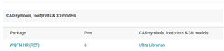
2.- CAD file (Ultra Librarian)

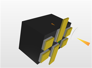
The following image shows the differences between some of the dimensions. The dimensions of the downloaded CAD file are written in red.

You can tell us which information is correct or if both are correct.

Thank you.

Best Regards,

Ricardo

  • Hi Ricardo,

    I checked this in the Altium footprint and the distance looks fine. Can you share some more details on where you are seeing this difference. 

    Best Regards,
    Arush

  • Arush,

    Thanks for checking the footprint.

    The footprint in the CAD file is very tight on 4 of the pads. It is well centered and the dimensions are correct, but I think the pads are too tight to hold the solder.

    The footprint I generated from the PDF has the wider PADs to hold the tin. But I really don't know which footprint is better to put on the PCB.

    Best Regards,

    Ricardo

  • Hi Ricardo,

    I don't fully follow you here. If the first one is correct then why do you have wider pads when you generated the second one using pdf dimensions. 

    When I checked the Altium footprint, it matched with the pdf dimensions. The datasheet (pdf) dimensions are the recommended ones and all the BLR testing is also done using these dimensions. So there were no inconsistencies for me. 

    Best Regards,
    Arush

  • Arush,

    For me the inconsistency is on page 23 of the data sheet (LAND PATTERN EXAMPLE, https://www.ti.com/lit/ds/symlink/tps22995.pdf#page=22). The 4 small pads in the CAD file have been generated in the same size as the pad dimensions of the component, however on page 23 there are other measurements for those pads. In larger components there is no problem with these differences, but in very small components like this one it can be important.

    Best Regards,

    Ricardo

  • Hi Ricardo,

    Thank you for patience.

    Pg #22 is device dimensions and Pg #23 is the land pattern dimension example (PCB footprint) so they won't be same. So these two won't be identical. I hope this clarifies the inconsistency which you mentioned.

    Best Regards,
    Arush