This thread has been locked.

If you have a related question, please click the "Ask a related question" button in the top right corner. The newly created question will be automatically linked to this question.

TPS92629-Q1: TPS92629-Q1

Part Number: TPS92629-Q1

Tool/software:

Hello I have a question regarding the TPS92629 Short to GND specification.

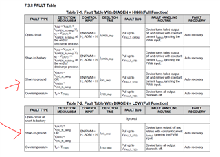
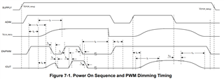
Short to GND deglith time defined at 125usec in the datasheet.
And I have concern of wrong detection at the start up.

Because if capacitive load is high and it takes more than 125usec to rise output voltage >1.24V, Wrong detection might be happened.
Does TPS92629 take preventive function of this situation ?

  • Hi Yoshihisa-san,

    What is your channel current and expected capacitance?

    The capacitor charging equation is I = C *dV/dt

    For the minimum output current of 5mA and a very large capacitance of 100nF, the channel will charge to 1.24V in less than 25μs.

    From this example, you can see that for any reasonable output capacitance and channel current the charging time will be far less than the deglitch time.

    Regards,

    Zach

  • Thanks for the reply.

    It's difficult to estimate expected capacitance.
    Because Output LED driver specification will be defined by user.
    My point of view, We need to expect very large capacitance like uF or larger level.

    As far as I checked TPS92629 EVM, It seems TPS92629 already implemented this preventive measure in design level.

  • Hi Yoshihisa-san,

    The TPS92629 auto-retry feature allows the device to auto-recover from any false short-to-ground detection that might occur due to a large capacitive load. See from figure 7-2, the 5mA retry current will constantly charge your μF capacitance even if the PWM signal is low. This allows the output voltage to quickly charge above the fault threshold.

    For most applications, I would not expect a large capacitance at the output as this will slow down the transient performance of the driver and reduce the linearity of PWM dimming.

    Regards,

    Zach

  • Thank you for your reply.

    Yes. I'm also aware and expect this feature.

    In addition,  I expect TPS92629 have mask feature at the rising timing.

    Following is the validation result of TSP92629.
    I connect output pin to GND and activated EN pin.
    It seems it takes 1.25msec to detect STG at fault pin.


    It means Short to GND diagnosis might be masked during the time of T(ADIM_current_rising) = 1msec.

  • Hi Yoshihisa-san,

    Can you also monitor the voltage at the PWM pin and the DIAGEN pin during your startup test?

    The PWM pin must be higher than VIH(PWM) and the DIAGEN pin must be higher than VIH(DIAGEN) in order for the diagnostics to be enabled.

    If you want to increase the time before the diagnostics are available in order to give your customer more time to charge a large output capacitance, you can place a capacitor in parallel with the lower resistor on the DIAGEN and size the RC time constant to your desired "no-fault" start-up time.

    Regards,

    Zach

  • Hello Zach-san,
    Thank you for your reply.

    I'm thining DAIGEN is not relevant for STG function.
    Adding capacitor does make sense ?


    And I also checked ADIM pin start up behaviour as same as EN pin.
    Result looks same as EN pin start up.

    Shoud I check my measurement set up again ?

  • Hi Yoshihisa-san,

    Good catch. You are correct, the DIAGEN pin is required high for the other faults but not for the short-to-ground fault. You may ignore my previous capacitor recommendation for this fault condition.

    I tested the fault timing on my EVM and I also found ~1.25ms delay for the fault to appear after driving EN/PWM pin high from the disabled state. Note that after the EN/PWM is low for ~20ms the device enters this disabled state and the Vcs_reg voltage is no longer maintained (see t8 below). When the device is enabled again, the Vcs_reg voltage must ramp up over 1ms slew time (see t7 below) and during this time the diagnostics are disabled. There is also the 125μs deglitch time and the 86μs enable time which brings the total fault delay very close to 1.25ms as measured.

    Essentially, when the device EN/PWM is low for more that 20ms, the device is disabled and is considered to be in "analog dimming mode" when it is enabled again. The "analog dimming mode" has a longer slew time that is optimized for EMC and large output capacitance. This is good for your application, as you mentioned conditions where a long start-up time is preferred due to a large output capacitance.

    Regards,

    Zach

  • Thank you for your quick reply.

    Understood.
    Now everything is clear for me.

    Considering the formula of I = C *dV/dt,
    Maximum capacitance should be around 4mF.

    It's very large and we can use TPS92629 in the application that is less than 4mF output capacitance.

    Thanks again.