TPS63020: Output discharge - current capability for PG pin

Part Number: TPS63020
Other Parts Discussed in Thread: TPS631011, TPS61033

Tool/software:

Hi TI team,

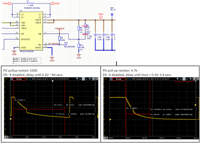
We are planning to implement a output discharge function using Power Good pin for the TPS63020.*
Could you indicate what is the maximum current capability? We couldn't find that information in the datasheet.

Thank you for your support.

Fabio Leitao

  • Hi  Fabio,

    Power Good pin are based on open-drain structure which means there is no source capability for this Pin. Mostly. there is resister connected to other sources, such as Vout or Vin.

    Then the maximum current capability is decided by this resister and VDD connencted.

    Recommend TPS631011, discharge function is integrated for this device.

    Regards

    Tao

  • Hi Tao,
    Thank you for reply.

    Yes, I understand that the pin is an open drain configuration (no source).
    What I mean is how low can that resistor be?
    in example, "the TPS61033 is an open drain NMOS architecture with up to 50 mA current capability". Is it similar?

    Thank you

  • Hi  Fabio,

    Oh, i got your point.

    The resistance of FET internal is from 4K-40K. Also, PG is low only when current limit triggered which means PG keep high in most conditions.

    Regards

    Tao

  • Hi Tao, 

    Sounds good.
    Thank you for the clarification.

    So when the converter is disabled (EN = low), to Power good is eventually pulled low.
    A rough estimate for calculating the discharge time (considering only the Power Good pin path) could be

    t = (R_pg + R_on_mosfet)* Cout * log(1/r),  where:
     - R_pg is the pull up resistor, 
     - R_on_mosfet can vary from 4k-40k, (40k worst case  scenario for the slowest discharge time)
     - Cout output capacitance,
     - r   ratio of the discharge terminal voltage

    Thanks,


    Fabio

  • Hi  Fabio,

    No, when device is disabled, the FET internal is off. So, i am afraid we are not able to use this Pin to discharge.

    Regards

    Tao

  • Hi Tao,

    Thank you for your message.
    I've performed the following measurements when the EN is set LOW for different pull up resistor value.
    During the discharge, the total output capacitance is around ~250uF.

    As it can be seen, changing the pull up resistor on the Power Good pin we can have different discharge delays. 

    For example, when using the 4.7k pull up, we measured around 5.6s, even though we were expecting just a slightly lower value. This might be due to the internal resistance of the N-FET that you mentioned (4k-40k?).   
    We just would like to get an idea of what would be the worst case scenario for the increased delay considering that internal resistance.

    Thank you for your support.

  • Hi Fabio,

    Seems PG is pulled low when device is disabled, or else, there should be no difference at the discharge time, right?

    Do Vin applied in your bench test?

    Yes, the resistance of FET internal is from 4K to 40K.

    Regards

    Tao

  •  - Yes, the PG is pulled low when the device is disabled.

    No, when device is disabled, the FET internal is off. So, i am afraid we are not able to use this Pin to discharge.

    So, this can indeed be used to discharge the output circuit when we disable the circuit.

    - Yes, VIN is constant 5.1V. Only the EN pin was toggled.

    I think it is clear. It just means that for our worst case scenario we'll have to consider 40k for the slowest discharge time.

    Thank you for your support,

    Fabio