Tool/software:
Hi all,
I have been researching the LLC SR driver. I've read the datasheet of UCD7138, and I have a question.
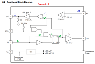
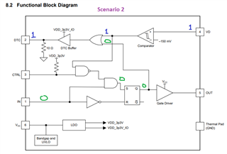
In "8.2 Functional Block Diagram (P.11)", there is an OR gate. It ORs the Q and comparator output, and the output is the DTC.
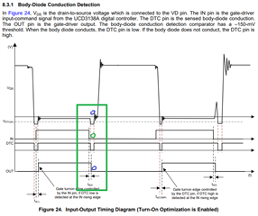
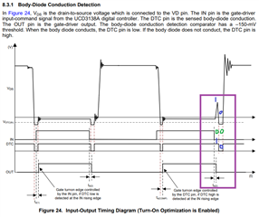
If Q goes to a Low level, the DTC should also be low. However, "Figure 24. Input-Output timing diagram" does not show the DTC as low when the OUT is low at the falling edge of the OUT.
Is the OR gate accurately expressing the operation of UCD7138?
Best regards,
YUKIOOYAMA