TPSM843620: Layout drawing

Part Number: TPSM843620

Tool/software:

 Hi,


  My customer has question on layout of this part. Becuase SMT factory asks 3 mils clearance on solder mask gap to prevent soldering connection.

  However, 

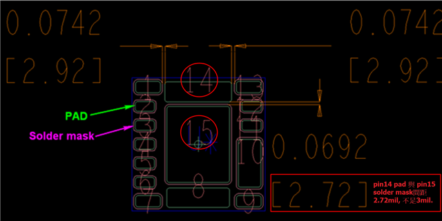
pin 14(VOUT) to pin 15(PAD/PGND) solder mask gap 2.72mil

pin1(FB) to pin 14(VOUT)  solder mask gap 2.92mil

pin13(SYNC/FSEL) to pin 14(VOUT)  solder mask gap 2.92mil

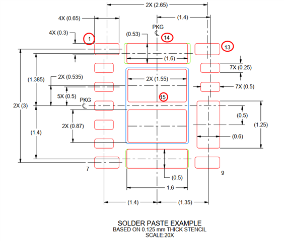
    Is this drawing on page 39 on data sheet correct? 

    Or how can customer to modify this 3 mil gap from each other pins?

  • The drawing on page 39 of datasheet is correct. 

    Pin 15 mask opening is smaller than pad in TI drawing.   In customer drawing the mask opening is greater than pad. 

    Pins 1 to 7, 9 to 13 in TI drawing the pad and mask opening are the same size.     In customer drawing, mask opening is greater than pad. 

    If customer wants to meet the 3mil requirement, update their footprint and mask to match the TI drawing.