This thread has been locked.

If you have a related question, please click the "Ask a related question" button in the top right corner. The newly created question will be automatically linked to this question.

TPS61096A: High consumption after few month without load

Part Number: TPS61096A

Tool/software:

Hello,

I'm electronic engineer for industry and I developped battery pack with a TPS61096A regulator last year. Since few weeks, we have seen suspect behavior of several products.

Our product consists of this regulator and our electronics with a microcontroller to manage Vout with set of resistors. Here is our schematic :

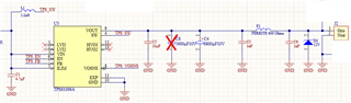
- Vin is 3.6V - cell is soldered in factory so product is always powered

- VOSNS and FB are connected to our set of resistors

- EN is connected to µC and always high

- level shifter is not used and not connected (I know it's not the best solution)

- C8 is not mounted and J2 is output

- Vout is between 5V and 6V according to µC algorithm

Here's the problem : when µC is sleeping, the pcb consumes <6µA and everything is ok. but on several products, average consumption is more than 70µA and up to 3mA for few products.

After investigation, I change TPS61096A by a brand-new component, and average consumption dropped under 6µA. So we suppose that regulator is faulty...

* These defective products were stored without load (quiescent current only <1µA) for almost 1 year, is regulator could be damaged in this configuration ?

* not connected pins of level shifter could damage regulator too ?

* can it be caused by ESD ?

I hope I shared enough information..

thanks for your help !

  • Hi Benjamin,

    Could you do one more experiment? Replace the brand-new TPS61096A with the abnormal TPS61096A, and measure the leakage again when µC is sleeping.

    Except the bigger leakage, have you observed any other abnormal behaviors? Can the Vout still be regulated correctly?

    - level shifter is not used and not connected (I know it's not the best solution)

    For the not-used function blocks, connecting the input pin to GND is usually better than leaving it floating. Well, for this device, I just checked with the designer and there should be no more risks to leave the LVI1 and LVI2 floating.

    * These defective products were stored without load (quiescent current only <1µA) for almost 1 year, is regulator could be damaged in this configuration ?

    Form the schematic, I see no concerns. And the device should work without spec degradation.

    Please provide the layout for check if available.

    * not connected pins of level shifter could damage regulator too ?

    No concerns for this device.

    * can it be caused by ESD ?

    Not likely.

    Regards

    Lei

  • Hi,

    Thanks for your post,

    We are currently preparing the products for testing with brand-new and abnormal components, I will have the results on Monday.

    We do not have observed other abnormal behavior, Vout remains stable.

    Here is the layout of tps61096A integration in our product :

    One more point I did not mention yet, all electronics and LTC cell are packed with two-component epoxy adhesive (spec file Specification résine UL94-V0 JD-320AB - EVE.pdf) could it modify component behavior or cause damage to it ?

    Thanks

    Benjamin

  • Hi,

    From the layout I see no concerns.

    could it modify component behavior or cause damage to it ?

    That may be the reason, but sorry I'm sure for this. If you have normally packed units, please also have a try.

    Regards

    Lei