Tool/software:
Hi,
This is a continuation of a related question. Could you please not close the forum so soon, since I need to post a new one every time? This is a question about Excel that I posted previously and got a response from. I've attached the Excel file that I got a response from last time.
Calculation results 10 2 24 (2).xlsx
Q1.
Please check the formula (35) and formula (64), as the way voltage is handled is different in each formula, and it may be reversed.
Formula (35)
"Voltage across drain-to-source (VdsQA) where COSS was measured, data sheet parameter / arbitrary voltage for which Coss_ave is to be calculated" states that VdsQA is the voltage when Coss was measured, and the arbitrary voltage for which Coss_ave is to be calculated.
Equation (64)
In "Voltage across FET QE and QF when they are off/Voltage where FET COSS is specified and tested in the FET data sheet", Vds_spec (the voltage where Coss is specified in the FET data sheet) and VdsQE (Vds when FET QE and QF are off) are used, and it seems that the denominator and numerator are reversed.
Regarding the treatment of fractions in equation (64), since Coss generally changes depending on the operating voltage of the device, the correct formula should be **(Vds_spec/VdsQE)^(1/2)**. By using this formula, the Coss of the FET QE should be closer to the expected value. In other words, is Coss_QE_AVG 1.45nF? Also, is the treatment of the voltage ratio in equation (64) reversed?
Q2.
Is my understanding of the following correct?
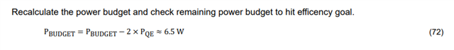
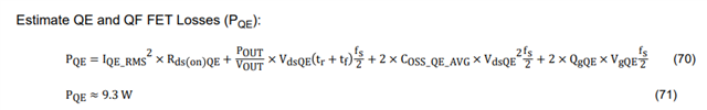
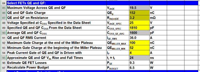
The loss calculated in equation (70) is calculated for one FET (e.g. QE or QF). In a full-bridge converter, two FETs, QE and QF, work as a pair, so the loss of both FETs must be considered. Therefore, in equation (72), this loss is doubled to obtain the total loss of QE and QF. In other words, the value of 14.4 W is the total loss of both QE and QF FETs.
Q3.
Equation (77) may need to be modified in the following two ways. Could you please confirm the following?
A. About POUT
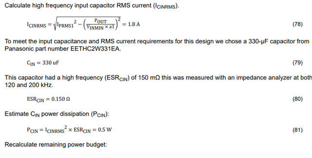
In equation (77), POUT (output power) is used to calculate the input capacitor capacitance, but in reality, the efficiency must be considered. Therefore, it is correct to use POUT / η. This allows the calculation to be based on the actual input power, including the system loss.
B. About VIN
In equation (77), VIN (input voltage) is used, but in reality, it is appropriate to use the minimum input voltage VINMIN. This is because the capacitance of the capacitor is most important when the input voltage is at its lowest.
If we calculate based on this correction, CIN will probably be 355uF or more.
Q4.
Equation (78) may need to be corrected in the following two points. Could you confirm the following?
C. Regarding a1
Equation (78) uses a1, but efficiency (η) should actually be used here. If the calculation is made without considering efficiency, the actual power loss cannot be correctly reflected, so a1 is incorrect and η is correct.
D. ICINRMS (Input Capacitor RMS Current)
When calculated using the corrected formula, it is considered reasonable that ICINRMS = 1.8A.
Furthermore, regarding the loss PCIN of the input capacitor, the loss is generally calculated as follows:
PCIN =ESR×I^2 CINRMS
Here, ESR is the equivalent series resistance of the input capacitor. If ICINRMS is 1.8A and ESR is an appropriate value, PCIN = 0.5W. Therefore, after correcting equation (78), ICINRMS becomes 1.8A, and based on that, the calculation result is thought to be 0.5W for the capacitor loss.
Q5.
I have a question about equation (84).
In fact, it is appropriate to use VINMIN for VINMAX used in equation (16) and equation (17). This is because the peak current is maximum at the minimum input voltage, which is the most severe operating condition.
Also, in equation (84), 2*fs (twice the switching frequency) must be corrected to the actual switching frequency fs. The 2 times in this part is incorrect, and the correct value is the simple switching frequency fs.
Based on the corrected equation from above, IP1 (peak current) is thought to be 3.3A. After correcting VINMIN and fs, the correct result is IP1 = 3.3A.
Is my understanding correct?
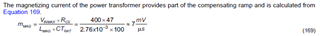
Q6.
Is the result of the calculation of equation (169) 68.1 * 10^3 V/s = 68.1 mV/us? Also, do I need to change VINMAX to 410V?
Q7.
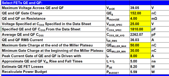
First, regarding QgQE in equation (70), does this refer to the same thing as QEg in equation (59)? Next, regarding VgQE, it does not seem to be clearly defined in the application note. I would like to know at what V the loss calculation result of 14.4W was obtained.
Thanks,
Conor