This thread has been locked.

If you have a related question, please click the "Ask a related question" button in the top right corner. The newly created question will be automatically linked to this question.

TPS53659: Not able to set VBOOT of Channel A: 1.8V

Part Number: TPS53659
Other Parts Discussed in Thread: CSD95492QVM

Tool/software:

Hi,

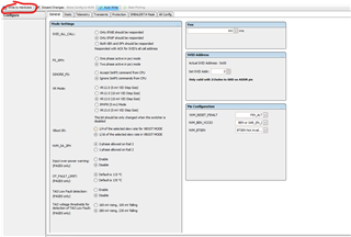
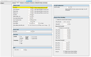
I have mentioned in earlier queries also. I have used TPS53659 SVID13 VR with Intel Xeon D1746 Processor. 

Now, I am trying to program the VR with TI POWER FUSION DESIGNER GUI. where I am not able to set the VBOOT Value of Channel A (1.8V) or above 1.520V. 

Please help me out with this. 

Thank You

Raj Kumar

  • Hi Raj,

    The default VOUT_MAX for channel A is 1.520 V, which is why you are not able to set your VBOOT for channel A above 1.52. To set the VBOOT to 1.8, you will first have to change the VOUT_MAX value for channel A. After VOUT_MAX has been changed, you should be able to change VBOOT.

    Regards,

    Maha

  • Hi Maha,

    Thank you the quick response.

    I tried to edit/change the VOUT_MAX value but still it is showing the error stating that "You must enter a number between 0.00 and 1.520V, inclusive".

    Please see the following steps-

    Step-1: I am running the GUI in Offline Mode.

    Step-2: I am setting the VR Mode: VR13.0 (10mV VID step size) for Rail#1 as shown in attached  screenshot-

    Step-3: Now, I am trying to change the value of VOUT_MAX as 1.8V and getting the error as shown is attached screen shot-

    Please suggest a solution.

    Also, You are requested share the "The Technical Reference Manual" that you referred in last reply. I have only datasheet, reference schematic and TI Fusion Manuals already.

    Thank You 

    Raj Kumar

  • Hi Raj, 

    Please make sure you "Write to Hardware" after changing the VR Mode to VR 13.0 (10 mV VID Step Size). After that, you should be able to change Vout Max to 1.8. (It goes up to 3.04V so you should have no issue there). 

    Please reach out to vr@list.ti.com for the full Technical Reference Manual for this device.

    Regards,

    Maha

  • Hi Maha, 

    Thank you for the help.

    I will try this method and let you know.

    Also, I have sent a mail on the contact ID, provided.

    Thank You

    Raj Kumar

  • Hi Maha,

    Now, I am able to edit the Vboot, Vmax and all other required parameters.

    I have a few things to ask about this-

    In my custom board design, TPS53659 is configured for (3 phases + 2 phases) where all three channels of Rail#1 is being used and only one out of two phases is used from Rail#2. I want to keep the Phase Shedding disabled for now and use CCM (continuous conduction mode).

    Imax from Channel A (Rail#1): 102A (Dynamic SVID)

    Imax from Channel B (Rail#2): 1.6A (Static SVID).

    Bases on the above operating conditions please help me out with following settings-

    1) My SVID Address is 0x00h and 0x01h for Channel A and B. Then What is the meaning of SVID_ALL_CALL setting & which is applicable in my case.

    2) I want to use CCM mode only for the time being, Shall I select "One phase active in PS1 mode".

    3) Can I choose "Ignore SetPS commands from CPU" ?

    Please refer below image-

    4) As I want to disable the Dynamic Phase Shedding (chosen option). then the Option "Disable 2 to 1 dynamic phase transitions means? it is related to Channel B (Rail#2) only? shall I choose CCM in 1-ph?

    5) As I have chosen the option "Disable dynamic phase shedding" then Do I have to provide the DPS phase shedding thresholds (like 3 to 2 or 2 to 1)? If yes, then What I have to set in phase4- to- 5 and phase-5 to 6 because I am using it in (phase 3 + phase 2) mode?

    Please refers below Image-

    Thank You

    Raj Kumar

  • Hi Raj,

    1. SVID ALL CALL is a SVID command in which you can send a command on SVID address 0xE or 0xF,  and we can decide if we want to listen to those or not through multiple different devices. If you are not intending to talk to multiple devices at once, then this setting does not matter.

    2. Because you will have DPS disabled, this does not matter. Just leave it as the default.

    3. Yes, just keep this as "Ignore".

    4. If you have DPS disabled (which you do), then this setting is also disabled and does not matter.

    5. No, if DPS is disabled then none of these settings matter. 

    Regards,

    Maha

  • Hi Maha,

    Thank you for the information.

    I got your answers. but I have small doubt on point (1).

    As you know, the SVID Address for this VR is 0x00h and 0x01h for channel A and channel B respectively which is configured via hardware only & Processor specific. 

    If the processor will be communicating with VR on SVID addresses 0x00h and 0x01h, then what will be the use of the 0x0Eh and 0x0Fh addresses?.

    New Doubt-

    I have not implemented the Input current (power) sensing circuitry. So, I want to use the Calculated IIN method. If I choose the option "Calculated IIN" then Do I need to provide the details in "calibration gain" and "calibration offset"?

    Please refer to the attached image-

    Thank You 

    Raj Kumar

  • Hi Raj,

    1. The two all-call addresses were assigned in order to allow grouping VRs on a shared VID bus into two different broadcast pools. For example, the slave address 0xEh could be assigned to all memory VRs and 0xFh could be assigned to all SoC VRs. Essentially, 0xEh and 0xFh are extra addresses that can be used to process commands, and we can decide if we want to listen to those or not through the GUI configuration.

    2. The calibration fields are for Sensed IIN, so if you are using Calculated, then you should not have to fill out those parameters.

    Regards,

    Maha

  • Hi Maha,

    Thank you so much for the reply!

    As you said that "we can decide if we want to listen to those or not through the GUI configuration".

    But I am not finding any such options where VR is not responding to any of the addresses. please refer to the below image-

    Thank You

    Raj Kumar

  • Hi Raj,

    I apologize for my wording. You actually cannot configure the device so that it does not respond to both addresses. However, this should not be an issue for you as long as you do not push any command to either of these addresses (0xEh or 0xFh). 

    Regards,

    Maha

  • Hi Maha,

    Thank you the clarifications! 

    Regarding the Compensation in transient response, I have gone through some design documents and guidelines. 

    But I am still uncertain about the correct values of AC_GAIN, AC_LL, INT_TIME & INTGAIN for my VR design. Do I have to try some combinations to fine tune the response? or there are some TI guidelines for this? 

    A couple of  small doubts- 

    Does Vout droop mean "DC Load Line (DCLL)"?

    Can I set Vout offset as 22mV which is Intel's VCCIN (AC+DC) tolerance?

    Thank You

    Raj Kumar

  • sorry forgot to attach reference screen shot-  Transient -> Compensation 

  • Hi Raj,

    1. For compensation, you will have to try some of your own values to properly tune your board. We do not have set guidelines on values because it depends on each board and layout.

    2. Yes, Vout Droop is the same thing as DC Load Line (DCLL).

    3. Vout offset is a fixed offset from the Vout command, the ripple offset of 22mV is the steady state spec based on the caps, number of phases etc. Can you explain why you are trying to put an offset for a tolerance?

  • Hi Maha,

    Thanks for the response:

    Please go through the below 5 points- 

    1) In my design, the SVID will be the sole controller of the VOUT. The PMBus will not be able to modify the VOUT.

    Given this setup, am I still required to fill in the values for VOUT Command, Margin High, and Margin Low?

    Additionally, are the settings for On/Off Operation, Margining, and Margin Fault Action also unnecessary? Please refer to the attached screenshot for clarification.

    2) I am unable to set the PIN_MAX value below 34W, and the II_OC_Warn_Limit cannot be set lower than 8A?

    3)  Does the TOA Low Fault Detection refer to the lower or negative temperature limit (for example, -40°C)? refer to the attached screen shot-

    4)  I’m a bit confused about the TMAX, Temperature Warning Limit, and Temperature Fault Limit. I have set the TMAX to 90°C, the Temperature Warning Limit to 105°C, and the Temperature Fault Limit to 115°C.

    Below are the 2 statements from the datasheet- 

    TMAX: - The temperature is sensed by the TSEN pin with connecting TAO pins of the CSD95492QVM power stages. The CSD95492QVM TAO pins are tied together so the hoter power stage temperature will be reported to the controller.

    OT_FAULT_LIMIT: - The OT_FAULT_LIMIT command sets the value of the temperature limit, in degrees Celsius, that causes an overtemperature fault condition when the sensed temperature from the external sensor exceeds this limit. 

    Now, Please tell me from which external temperature sensor, this OT_FAULT_LIMIT & OT_WARN_LIMIT limits to be compared? because I have not connected any external temperature sensor except Power Stage's integrated sensor?. 

    5) How TMAX value is related to OT_FAULT_LIMIT & OT_WARN_LIMIT values? refer to the attached screen shot-

    Thank You

    Raj Kumar

  • Hi Raj,

    1.  It is good to have the VOUT Command set to Vboot from the Platform Design Guide. You should have ON/OFF config set to whatever you need (always converting, control pin, etc). The margin commands depend on whether or not you want to use margining. Margin high/low will reset to 0 because they do not have NVM.

    2.  34 W is the minimum for PIN_MAX and 8A is the minimum for IIN_OC_WARN_LIMIT. These cannot be lowered.

    3. TAO low fault limit sets how low the TAO signal must be for it to register as a fault as opposed to just a temperature reading. It does not change the mV value for -40C in any way. It just affects when the controller decides a PS is holding TAO low as opposed to it just being cold temp.

    4. The external sensor being referred to is just the power stage temperature sensor. OT_FAULT_LIMIT and OT_FAULT_WARN are both compared to TAO from the power stage.

    5. TMAX is only for SVID and is the threshold that triggers the VRHOT pin. OT_FAULT_LIMIT and OT_WARN_LIMIT are PMBus. TMAX is usually lower than OT_FAULT and OT_WARN limits. 

  • Hi Maha,

    Thank you for the detailed explanation.

    I understand most of your points, but I have a slight confusion regarding the VOUT Command and Margining.

    1. I’m uncertain about how the VOUT Command and Margining work. Is Margining still applicable if the SVID interface is only controlling the VID (output voltage)? If so, could you please help clarify this?

    For example, let’s assume the required Vboot is 1.8V, and the SVID range is 1.5V to 2.0V.

    • Does this mean that the Margin High would be set to 2.0V and the Margin Low to 1.5V?
    • If I select “HIGH” for Margining, would the converter turn off if the output voltage exceeds 2.0V?

    Am I interpreting this correctly, or is there something I’m missing?

    Thanks again for your help!

    Thank You

    Raj Kumar

  • Hi Raj,

    What you are describing is VMAX. Margining is just used to switch between different Vouts. 

    Regards,

    Maha

  • Hi Maha,

    I have received the Intel Xeon Based our custom assembled board. 

    As per board bring-up plan. I am planning to configure the NVM of TPS53659 for VCCIN & 1V8_AUX supply. 

    Since There is no provision to isolate VR's output from target load (Intel Xeon), Please look at the requirements and fusion generated files and review them if it is possible. 

    Requirements: 

    Channel A (Rail#1): -

    Active Phases- 3 nos (always, without phase sheding)

    TDC Current- 39A (or 13A per phase)

    Max Current- 102A (or 34A per phase)

    VBOOT- 1.8V

    VID Range- 1.5V to 2.0V  (dynamic VID)

    Switching Frequency- 850KHz

    Channel B (Rail#2): -

    Active channel- 1 

    TDC Current- 1.8A

    Max current- 1.8A

    VBOOT- 1.8V

    VID Range - Static VID (always 1.8V)

    Switching Frequency- 850KHz

    based on the above requirements, Please review the fusion generated files. 

    Please suggest us if there is any hazard to target device (Intel Xeon) if I flash this file to VR NVM? 

    Is this configuration safe to program?

    devices_report.xls

    I am not able to attach the TIFSP file. kindly let me know if you require anything else regarding this.

    Thank You

    Raj Kumar

  • Hi Raj,

    The values that you have sent look compatible with our controller. I cannot tell you if there would be any hazard to Intel Xeon, as that would depend on the platform's specifications. 

    Regards,

    Maha