This thread has been locked.

If you have a related question, please click the "Ask a related question" button in the top right corner. The newly created question will be automatically linked to this question.

TPS55288: Calculation of IC temperature rise by considering the impact of exposed pad, thermal vias etc

Part Number: TPS55288

Tool/software:

I'm following the AN2020 TI application note & making a template so as to predict the accurate IC temperature rise in our worst case scenario calculation.  I've calculated the required rtja w.r.t copper, exposed pad & thermal vias seperately but I need a formula or technique which will combine all the rtja & give the final result.  

 I've attached the template with some rough calculation as per one of our board.  

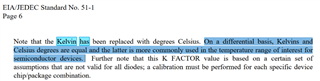
 Also, I'm a bit confused on the following statement in the EIA/JESD51-1 standard: 


  • Hi Santhosh,

    Thanks for sharing the wonderful AppNote. But from the app note, it mainly discussed about the tips for designing the PCB to help with the thermal performance, and doesn't tell how to get the final result, sorry I can't help you that.

    We used to use the modern finite element analysis software to get the board RθJA value. The theoretical calculation is difficult to calibrate the real test result and is very difficult in calculation.

    BRs,

    Bryce